-
SNx4HC273 Octal D-Type Flip-Flops With Clear
- 1 Features
- 2 Applications
- 3 Description
- 4 Revision History
- 5 Pin Configuration and Functions
-
6 Specifications
- 6.1 Absolute Maximum Ratings
- 6.2 ESD Ratings – SN74HC273
- 6.3 Recommended Operating Conditions
- 6.4 Thermal Information
- 6.5 Electrical Characteristics
- 6.6 Electrical Characteristics – SN54HC273
- 6.7 Electrical Characteristics – SN74HC273
- 6.8 Timing Requirements
- 6.9 Timing Requirements – SN54HC273
- 6.10 Timing Requirements – SN74HC273
- 6.11 Switching Characteristics
- 6.12 Switching Characteristics – SN54HC273
- 6.13 Switching Characteristics – SN74HC273
- 6.14 Operating Characteristics
- 6.15 Typical Characteristics
- 7 Parameter Measurement Information
- 8 Detailed Description
- 9 Application and Implementation
- 10Power Supply Recommendations
- 11Layout
- 12Device and Documentation Support
- 13Mechanical, Packaging, and Orderable Information
- IMPORTANT NOTICE
Package Options
Refer to the PDF data sheet for device specific package drawings
Mechanical Data (Package|Pins)
- DB|20
- NS|20
- N|20
- DW|20
- PW|20
Thermal pad, mechanical data (Package|Pins)
Orderable Information
DATA SHEET
SNx4HC273 Octal D-Type Flip-Flops With Clear
1 Features
- Wide operating voltage range of 2 V to 6 V
- Outputs can drive up to 10 LSTTL loads
- Low power consumption, 80-µA maximum ICC
- Typical tpd = 12 ns
- ±4-mA output drive at 5 V
- Low input current of 1-µA maximum
- Contain eight flip-flops with single-rail outputs
- Direct clear input
- Individual data input to each flip-flop
- On products compliant to MIL-PRF-38535,
all parameters are tested unless otherwise noted. On all other products, production processing does not necessarily include testing of all parameters.
2 Applications
- Buffer or storage registers
- Shift registers
- Pattern generators
3 Description
The SNx4HC273 devices are positive-edge-triggered D-type flip-flops with a direct active low clear ( CLR) input.
Information at the data (D) inputs meeting the setup time requirements is transferred to the Q outputs on the positive-going edge of the clock (CLK) pulse. Clock triggering occurs at a particular voltage level and is not related directly to the transition time of the positive-going pulse. When CLK is at either the high or low level, the D input has no effect at the output.
Device
Information(1)
| PART NUMBER | PACKAGE (PINS) | BODY SIZE (NOM) |
|---|---|---|
| SN54HC273J | CDIP (20) | 24.20 mm × 6.92 mm |
| SN54HC273W | CFP (20) | 13.09 mm × 6.92 mm |
| SN54HC273FK | LCCC (20) | 8.89 mm × 8.89 mm |
| SN74HC273D | SOIC (20) | 12.80 mm × 7.50 mm |
| SN74HC273DB | SSOP (20) | 7.20 mm × 5.30 mm |
| SN74HC273NS | SO (20) | 12.60 mm × 5.30 mm |
| SN74HC273N | PDIP (20) | 24.33 mm × 6.35 mm |
| SN74HC273PW | TSSOP (20) | 6.50 mm × 4.40 mm |
(1) For all available packages, see the orderable addendum at the end of the data sheet.
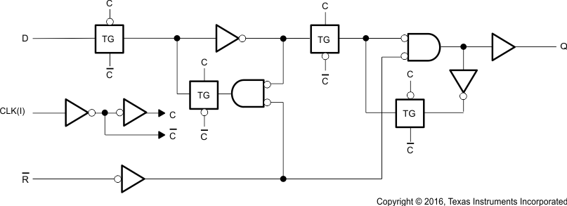
 Functional Block Diagram