SCLS040G December 1982 – March 2015 SN74HC594
UNLESS OTHERWISE NOTED, this document contains PRODUCTION DATA.
- 1 Features
- 2 Applications
- 3 Description
- 4 Revision History
- 5 Pin Configuration and Functions
-
6 Specifications
- 6.1 Absolute Maximum Ratings
- 6.2 ESD Ratings
- 6.3 Recommended Operating Conditions
- 6.4 Thermal Information
- 6.5 Electrical Characteristics
- 6.6 Switching Characteristics: CL = 50 pF
- 6.7 Switching Characteristics: CL = 150 pF
- 6.8 Timing Requirements
- 6.9 Operating Characteristics
- 6.10 Typical Characteristics
- 7 Parameter Measurement Information
- 8 Detailed Description
- 9 Application and Implementation
- 10Power Supply Recommendations
- 11Layout
- 12Device and Documentation Support
- 13Mechanical, Packaging, and Orderable Information
Package Options
Refer to the PDF data sheet for device specific package drawings
Mechanical Data (Package|Pins)
- DW|16
- N|16
- D|16
Thermal pad, mechanical data (Package|Pins)
- DW|16
Orderable Information
1 Features
- Wide Operating Voltage Range of 2 V to 6 V
- High-Current Outputs Can Drive up to
15 LSTTL Loads - Low Power Consumption, 80-µA Maximum ICC
- Typical tpd = 15 ns
- ±6-mA Output Drive at 5 V
- Low Input Current of 1 µA Maximum
- 8-Bit Serial-In, Parallel-Out Shift Registers With Storage
- Independent Direct Overriding Clears on Shift and Storage Registers
- Independent Clocks for Both Shift and
Storage Registers
2 Applications
- Pro Audio Mixer
- Elevators and Escalators
- Human Machine Interface (HMI): Industrial Monitor
- Entertainment Systems
- Grid Infrastructure: Grid Control
- Access Control and Security: DVR and DVS
3 Description
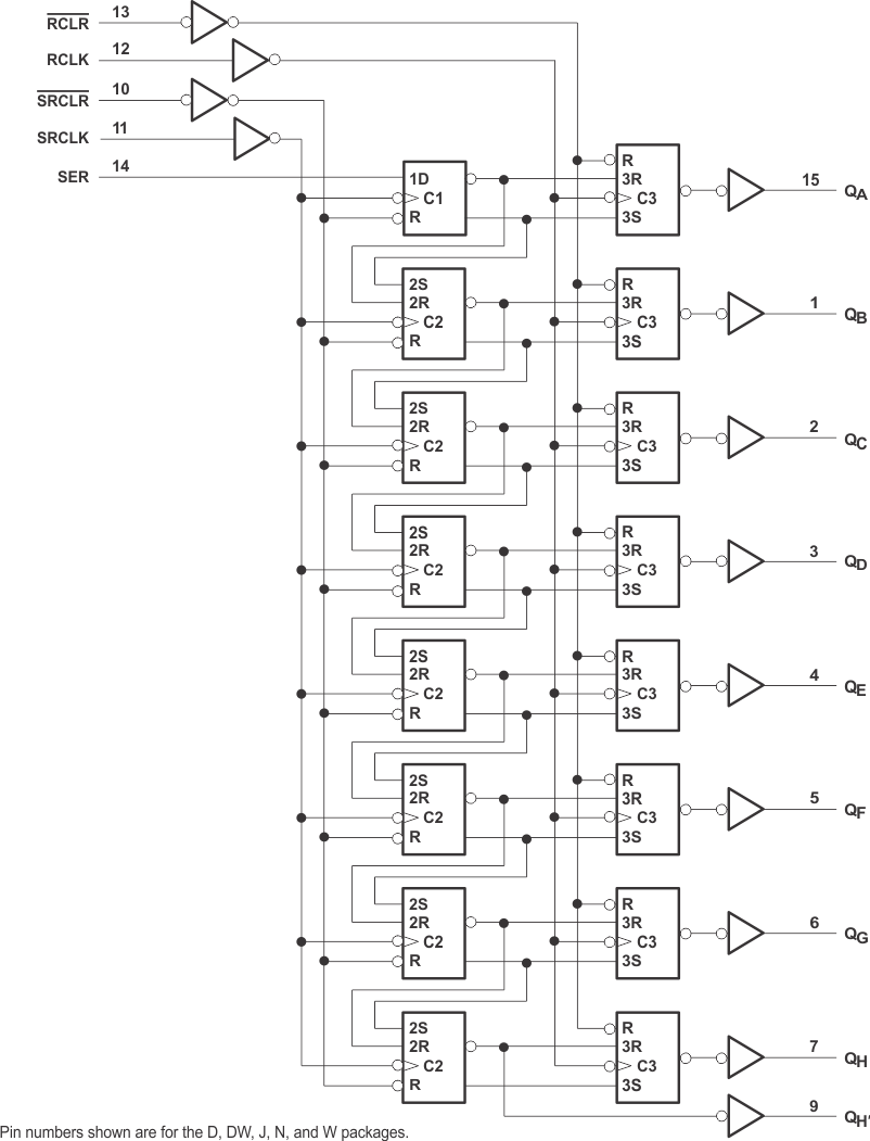
The SNx4HC594 devices contain an 8-bit serial-in, parallel-out shift register that feeds an 8-bit D-type storage register. Separate clocks and direct overriding clear (RCLR, SRCLR) inputs are provided on both the shift and storage registers. A serial (QH’) output is provided for cascading purposes.
Both the shift register (SRCLK) and storage register (RCLK) clocks are positive edge triggered. If both clocks are connected together, the shift register always is one count pulse ahead of the storage register.
The parallel (QA − QH) outputs have high-current capability. QH’ is a standard output.
Device Information(1)
| PART NUMBER | PACKAGE | BODY SIZE (NOM) |
|---|---|---|
| SN74HC594 | PDIP (16) | 19.30 mm × 6.35 mm |
| SOIC (16) | 9.00 mm × 9.00 mm | |
| 10.30 mm × 7.50 mm |
- For all available packages, see the orderable addendum at the end of the datasheet.
Logic Diagram (Positive Logic)
