-
SN74LV174A Hex D-Type Flip-Flops With Clear
- 1 Features
- 2 Applications
- 3 Description
- 4 Revision History
- 5 Pin Configuration and Functions
-
6 Specifications
- 6.1 Absolute Maximum Ratings
- 6.2 ESD Ratings
- 6.3 Recommended Operating Conditions
- 6.4 Thermal Information
- 6.5 Electrical Characteristics
- 6.6 Timing Requirements, VCC = 2.5 V ± 0.2 V
- 6.7 Timing Requirements, VCC = 3.3 V ± 0.3 V
- 6.8 Timing Requirements, VCC = 5 V ± 0.5 V
- 6.9 Switching Characteristics, VCC = 2.5 V ± 0.2 V
- 6.10 Switching Characteristics, VCC = 3.3 V ± 0.3 V
- 6.11 Switching Characteristics, VCC = 5 V ± 0.5 V
- 6.12 Noise Characteristics
- 6.13 Operating Characteristics
- 6.14 Typical Characteristics
- 7 Parameter Measurement Information
- 8 Detailed Description
- 9 Application and Implementation
- 10Device and Documentation Support
- 11Mechanical, Packaging, and Orderable Information
- IMPORTANT NOTICE
Package Options
Refer to the PDF data sheet for device specific package drawings
Mechanical Data (Package|Pins)
- PW|16
- NS|16
- D|16
- DGV|16
Thermal pad, mechanical data (Package|Pins)
Orderable Information
DATA SHEET
SN74LV174A Hex D-Type Flip-Flops With Clear
1 Features
- VCC operation of 2 V to 5.5
- Maximum tpd of 7.5 ns at 5 V
- Typical VOLP (output ground bounce)
< 0.8 V at VCC = 3.3 V, TA = 25°C - Typical VOHV (output VOH
undershoot)
> 2.3 V at VCC = 3.3 V, TA = 25°C - Ioff supports partial-power-down mode operation
- Supports mixed-mode voltage operation
on all ports - Latch-up performance exceeds 250 mA per JESD 17
3 Description
The 'LV174A devices are hex D-type flip-flops designed for 2 V to 5.5 V VCC operation.
Package Information(1)
| PART NUMBER | PACKAGE | BODY SIZE (NOM) |
|---|---|---|
| SN74LV174A | DGV (TVSOP, 16) | 4.00 mm × 3.50 mm |
| PW (TSSOP, 16) | 5.00 mm × 4.40 mm | |
| NS (SO, 16) | 10.20 mm × 5.30 mm | |
| D (SOIC, 16) | 9.00 mm × 3.90 mm |
(1) For all available packages, see the orderable addendum at the end of the data sheet.
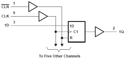
 Logic Diagram (Positive Logic)