-
SN74LV244A-Q1 Automotive Octal Buffers and Drivers With 3-State Outputs
- 1 Features
- 2 Applications
- 3 Description
- 4 Revision History
- 5 Pin Configuration and Functions
-
6 Specifications
- 6.1 Absolute Maximum Ratings
- 6.2 ESD Ratings
- 6.3 Recommended Operating Conditions
- 6.4 Thermal Information
- 6.5 Electrical Characteristics
- 6.6 Switching Characteristics, VCC = 2.5 V ± 0.2 V
- 6.7 Switching Characteristics, VCC = 3.3 V ± 0.3 V
- 6.8 Switching Characteristics, VCC = 5 V ± 0.5 V
- 6.9 Noise Characteristics
- 6.10 Operating Characteristics
- 6.11 Typical Characteristics
- 7 Parameter Measurement Information
- 8 Detailed Description
- 9 Application and Implementation
- 10Device and Documentation Support
- 11Mechanical, Packaging, and Orderable Information
- IMPORTANT NOTICE
Package Options
Mechanical Data (Package|Pins)
Thermal pad, mechanical data (Package|Pins)
- RKS|20
Orderable Information
DATA SHEET
SN74LV244A-Q1 Automotive Octal Buffers and Drivers With 3-State Outputs
1 Features
- AEC-Q100 qualified for automotive applications:
- Device temperature grade 1:
- 40°C to + 125°C, TA
- Device HBM ESD Classification Level 2
- Device CDM ESD Classification Level C6
- Device temperature grade 1:
- Available in Section 8.3.4 QFN (WRKS) package
- 2 V to 5.5 V VCC operation
- Maximum tpd of 6.5 ns at 5 V
- Supports mixed-mode voltage operation on all ports
- Ioff supports partial-power-down mode operation
- Latch-up performance exceeds 250 mA per JESD 17
3 Description
The SN74LV244A-Q1 octal buffers and line drivers are designed for 2 V to 5.5 V VCC operation.
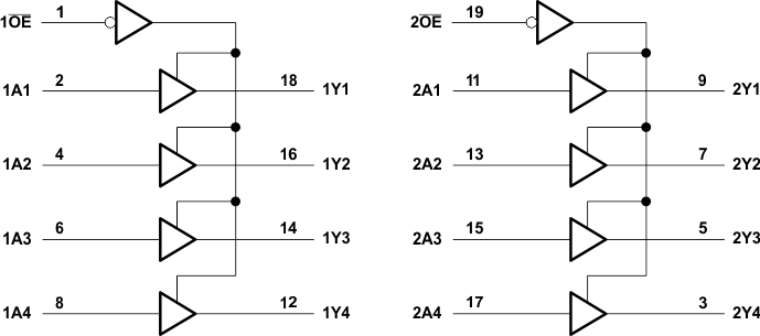
The device is configured into two banks of four drivers, each controlled by its own output enable pin. This device is fully specified for partial-power-down applications using Ioff. The Ioff circuitry disables the outputs, preventing damaging current backflow through the devices when they are powered down.
Pacakge
Information(1)
| PART NUMBER | PACKAGE | BODY SIZE (NOM) |
|---|---|---|
| SN74LV244A-Q1 | WRKS (WQFN, 20) | 4.50 mm × 2.50 mm |
| DGS (VSSOP, 20) | 5.10 mm × 3.00 mm |
(1) For all available packages, see the orderable addendum at the end of the data sheet.
 Logic Diagram (Positive Logic)