-
SN74LVCC4245A Octal Dual-Supply Bus Transceiver With Configurable Output Voltage and 3-State Outputs
- 1 Features
- 2 Applications
- 3 Description
- 4 Revision History
- 5 Pin Configuration and Functions
- 6 Specifications
- 7 Power-Up Consideration
- 8 Parameter Measurement Information For A to B VCCA = 4.5 V to 5.5 V and VCCB = 2.7 V to 3.6 V
- 9 Parameter Measurement Information For A to B VCCA = 4.5 V to 5.5 V and VCCB = 3.6 V to 5.5 V
- 10Parameter Measurement Information For B to A VCCA = 4.5 V to 5.5 V and VCCB = 2.7 V to 3.6 V
- 11Parameter Measurement Information For B to A VCCA = 4.5 V to 5.5 V and VCCB = 3.6 V to 5.5 V
- 12Detailed Description
- 13Application and Implementation
- 14Power Supply Recommendations
- 15Layout
- 16Device and Documentation Support
- 17Mechanical, Packaging, and Orderable Information
- IMPORTANT NOTICE
Package Options
Mechanical Data (Package|Pins)
Thermal pad, mechanical data (Package|Pins)
- DW|24
Orderable Information
SN74LVCC4245A Octal Dual-Supply Bus Transceiver With Configurable Output Voltage and 3-State Outputs
1 Features
- Bidirectional voltage translator
- 4.5 V to 5.5 V on A port and
2.7 V to 5.5 V on B port - Control inputs VIH and VIL levels are referenced to VCCA voltage
- Latch-up performance exceeds 250 mA
per JESD 17 - ESD protection exceeds JESD 22
- 2000-V Human-Body Model (A114-A)
- 1000-V Charged-Device Model (C101)
2 Applications
- Level translation
- Personal electronics
- Industrial
- Enterprise
- Telecom
3 Description
This 8-bit (octal) noninverting bus transceiver uses two separate power-supply rails. The A port, VCCA, is dedicated to accepting a 5-V supply level, and the configurable B port, which is designed to track VCCB, accepts voltages from 3 V to 5 V. This allows for translation from a 3.3-V to a 5-V environment and vice versa.
The SN74LVCC4245A device is designed for asynchronous communication between data buses. The SN74LVCC4245A device transmits data from the A bus to the B bus or from the B bus to the A bus, depending on the logic level at the direction-control (DIR) input. The output-enable (OE) input can be used to disable the device so the buses effectively are isolated. The control circuitry (DIR, OE) is powered by VCCA.
| PART NUMBER | PACKAGE | BODY SIZE (NOM) |
|---|---|---|
| SN74LVCC4245A | DB (SSOP, 24) | 8.20 mm × 5.30 mm |
| DW (SOIC, 24) | 15.40 mm × 7.50 mm | |
| NS (SOP, 24) | 15.00 mm × 5.30 mm | |
| PW (TSSOP, 24) | 7.80 mm × 4.40 mm |
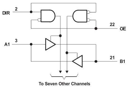
 Logic Diagram (Positive Logic)
4 Revision History
Changes from Revision M (March 2005) to Revision N (December 2022)
5 Pin Configuration and Functions
| PIN | TYPE(1) | DESCRIPTION | |
|---|---|---|---|
| NAME | NO. | ||
| VCCA | 1 | — | A port power |
| DIR | 2 | I | Dir input |
| A1 | 3 | I/O | A1 port |
| A2 | 4 | I/O | A2 port |
| A3 | 5 | I/O | A3 port |
| A4 | 6 | I/O | A4 port |
| A5 | 7 | I/O | A5 port |
| A6 | 8 | I/O | A6 port |
| A7 | 9 | I/O | A7 port |
| A8 | 10 | I/O | A8 port |
| GND | 11 | — | Ground |
| GND | 12 | — | |
| GND | 13 | — | |
| B8 | 14 | I/O | B8 port |
| B7 | 15 | I/O | B7 port |
| B6 | 16 | I/O | B6 port |
| B5 | 17 | I/O | B5 port |
| B4 | 18 | I/O | B4 port |
| B3 | 19 | I/O | B3 port |
| B2 | 20 | I/O | B2 port |
| B1 | 21 | I/O | B1 port |
| OE | 22 | I | Output Enable active low |
| NC | 23 | — | Unconnected |
| VCCB | 24 | — | B port power |