SLAS846A May 2012 – March 2015 TAS5614LA
PRODUCTION DATA.
- 1 Features
- 2 Applications
- 3 Description
- 4 Revision History
- 5 Pin Configuration and Functions
- 6 Specifications
-
7 Detailed Description
- 7.1 Overview
- 7.2 Functional Block Diagrams
- 7.3
Feature Description
- 7.3.1 Power Supplies
- 7.3.2 System Power-Up and Power-Down Sequence
- 7.3.3 Start-up and Shutdown Ramp Sequence
- 7.3.4 Unused Output Channels
- 7.3.5 Device Protection System
- 7.3.6 Pin-to-Pin Short-Circuit Protection (PPSC)
- 7.3.7 Overtemperature Protection
- 7.3.8 Overtemperature Warning, OTW
- 7.3.9 Undervoltage Protection (UVP) and Power-On Reset (POR)
- 7.3.10 Error Reporting
- 7.3.11 Fault Handling
- 7.3.12 Device Reset
- 7.4 Device Functional Modes
- 8 Application and Implementation
- 9 Power Supply Recommendations
- 10Layout
- 11Device and Documentation Support
- 12Mechanical, Packaging, and Orderable Information
Package Options
Mechanical Data (Package|Pins)
- DDV|44
Thermal pad, mechanical data (Package|Pins)
- DDV|44
Orderable Information
1 Features
- PurePath™ HD Integrated Feedback Provides:
- Preclipping Output for Control of a Class-G Power Supply
- Reduced Heat Sink Size due to use of 60-mΩ Output MOSFET With > 90% Efficiency at Full Output Power
- Output Power at 10%THD+N
- 150-W and 4-Ω BTL Stereo Configuration
- 300-W and 2-Ω in PBTL Mono Configuration
- Output Power at 1%THD+N
- 125-W and 4-Ω BTL Stereo Configuration
- 65-W and 8-Ω BTL Stereo Configuration
- Click- and Pop-Free Start-up
- Error Reporting Self-Protected Design With UVP, Overtemperature, and Short-Circuit Protection
- EMI Compliant When Used With Recommended System Design
- 44-Pin HTSSOP (DDV) Package for Reduced Board Size
2 Applications
- Blu-ray™ and DVD Receivers
- High-Power Sound Bars
- Powered Subwoofer and Active Speakers
- Mini Combo Systems
3 Description
The TAS5614LA device is a feature optimized class-D power amplifier based on the TAS5614LA.
The TAS5614LA uses large MOSFETs for improved power efficiency and a novel gate drive scheme for reduced losses in idle and at low output signals leading to reduced heat sink size.
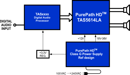
The unique preclipping output signal can be used to control a class-G power supply. This combined with the low idle loss and high power efficiency of the TAS5614LA leads to industry-leading levels of efficiency ensuring a super “green” system.
The TAS5614LA uses constant voltage gain. The internally matched gain resistors ensure a high Power Supply Rejection Ratio giving an output voltage only dependent on the audio input voltage and free from any power supply artifacts.
The high integration of the TAS5614LA makes the amplifier easy to use; and, using TI’s reference schematics and PCB layouts leads to fast design in time. The TAS5614LA is available in the space-saving, surface-mount, 44-pin HTSSOP package.
Device Information(1)
| PART NUMBER | PACKAGE | BODY SIZE (NOM) |
|---|---|---|
| TAS5614LA | HTSSOP (44) | 14.00 mm × 6.10 mm |
- For all available packages, see the orderable addendum at the end of the data sheet.
Typical TAS5614LA Application Block Diagram
