SLASE77A March 2016 – March 2016 TAS5733L
PRODUCTION DATA.
- 1 Features
- 2 Applications
- 3 Description
- 4 Revision History
- 5 Pin Configuration and Functions
-
6 Specifications
- 6.1 Absolute Maximum Ratings
- 6.2 ESD Ratings
- 6.3 Recommended Operating Conditions
- 6.4 Thermal Characteristics
- 6.5 Electrical Characteristics
- 6.6 Speaker Amplifier Characteristics
- 6.7 Protection Characteristics
- 6.8 Master Clock Characteristics
- 6.9 I²C Interface Timing Requirements
- 6.10 Serial Audio Port Timing Requirements
- 6.11 Typical Characteristics - Stereo BTL Mode
- 6.12 Typical Characteristics - Mono PBTL Mode
-
7 Detailed Description
- 7.1 Overview
- 7.2 Functional Block Diagram
- 7.3 Audio Signal Processing Overview
- 7.4 Feature Description
- 7.5 Device Functional Modes
- 7.6 Programming
- 7.7
Register Maps
- 7.7.1 Register Summary
- 7.7.2
Detailed Register Descriptions
- 7.7.2.1 Clock Control Register (0x00)
- 7.7.2.2 Device ID Register (0x01)
- 7.7.2.3 Error Status Register (0x02)
- 7.7.2.4 System Control Register 1 (0x03)
- 7.7.2.5 Serial Data Interface Register (0x04)
- 7.7.2.6 System Control Register 2 (0x05)
- 7.7.2.7 Soft Mute Register (0x06)
- 7.7.2.8 Volume Registers (0x07, 0x08, 0x09)
- 7.7.2.9 Volume Configuration Register (0x0E)
- 7.7.2.10 Modulation Limit Register (0x10)
- 7.7.2.11 Interchannel Delay Registers (0x11, 0x12, 0x13, and 0x14)
- 7.7.2.12 PWM Shutdown Group Register (0x19)
- 7.7.2.13 Start/Stop Period Register (0x1A)
- 7.7.2.14 Oscillator Trim Register (0x1B)
- 7.7.2.15 BKND_ERR Register (0x1C)
- 7.7.2.16 Input Multiplexer Register (0x20)
- 7.7.2.17 PWM Output MUX Register (0x25)
- 7.7.2.18 AGL Control Register (0x46)
- 7.7.2.19 PWM Switching Rate Control Register (0x4F)
- 7.7.2.20 Bank Switch and EQ Control (0x50)
-
8 Application and Implementation
- 8.1 Application Information
- 8.2
Typical Applications
- 8.2.1
Stereo Bridge Tied Load Application
- 8.2.1.1 Design Requirements
- 8.2.1.2 Detailed Design Procedure
- 8.2.1.3 Application Performance Plots
- 8.2.2 Mono Parallel Bridge Tied Load Application
- 8.2.1
Stereo Bridge Tied Load Application
- 9 Power Supply Recommendations
- 10Layout
- 11Device and Documentation Support
- 12Mechanical, Packaging, and Orderable Information
Package Options
Mechanical Data (Package|Pins)
- DCA|48
Thermal pad, mechanical data (Package|Pins)
- DCA|48
Orderable Information
1 Features
- Audio Input/Output
- One-Stereo Serial Audio Input
- Supports 44.1-kHz and 48-kHz Sample Rates (LJ/RJ/I²S)
- Supports 3-Wire I²S Mode (no MCLK required)
- Automatic Audio Port Rate Detection
- Supports BTL and PBTL Configuration
- POUT = 10 W @ 10% THD+N
- PVDD = 12 V, 8 Ω, 1 kHz
- Audio/PWM Processing
- Independent Channel Volume Controls With Gain of 24 dB to Mute in 0.125-dB Steps
- Programmable Three-Band Automatic Gain Limiting (AGL)
- 20 Programmable Biquads for Speaker EQ and Other Audio-Processing Features
- General Features
- 104-dB SNR, A-Weighted, Referenced to Full Scale (0 dB)
- I²C Serial Control Interface w/ two Addresses
- Thermal, Short-Circuit, and Undervoltage Protection
- Up to 90% Efficient
- AD, BD, and Ternary Modulation
- PWM Level Meter
2 Applications
- LCD TV, LED TV
- Low-Cost Audio Equipment
3 Description
The TAS5733L device is an efficient, digital-input audio amplifier for driving stereo speakers configured as a bridge tied load (BTL). In parallel bridge tied load (PBTL) in can produce higher power by driving the parallel outputs into a single lower impedance load. One serial data input allows processing of up to two discrete audio channels and seamless integration to most digital audio processors and MPEG decoders. The device accepts a wide range of input data and data rates. A fully programmable data path routes these channels to the internal speaker drivers.
The TAS5733L device is a slave-only device receiving all clocks from external sources. The TAS5733L device operates with a PWM carrier between a 384-kHz switching rate and a 288-kHz switching rate, depending on the input sample rate. Oversampling combined with a fourth-order noise shaper provides a flat noise floor and excellent dynamic range from 20 Hz to 20 kHz.
Device Information(1)
| PART NUMBER | PACKAGE | BODY SIZE (NOM) |
|---|---|---|
| TAS5733L | HTSSOP (48) | 12.50 mm × 6.10 mm |
- For all available packages, see the orderable addendum at the end of the data sheet.
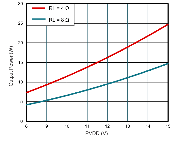
Power vs PVDD

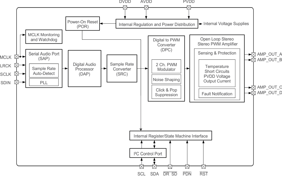
Simplified Block Diagram
