-
TAS5753MD 20-W I²S Input Class-D Amplifier With Digital Audio Processor and DirectPath™ HP and Line Driver
- 1 Features
- 2 Applications
- 3 Description
- 4 Revision History
- 5 Pin Configuration and Functions
-
6 Specifications
- 6.1 Absolute Maximum Ratings
- 6.2 ESD Ratings
- 6.3 Recommended Operating Conditions
- 6.4 Thermal Characteristics
- 6.5 Electrical Characteristics
- 6.6 Speaker Amplifier Characteristics in All Modes
- 6.7 Speaker Amplifier Characteristics in Stereo Bridge Tied Load (BTL) Mode
- 6.8 Speaker Amplifier Characteristics in Stereo Post-Filter Parallel Bridge Tied Load (Post-Filter PBTL) Mode
- 6.9 Headphone Amplifier and Line Driver Characteristics
- 6.10 Protection Circuitry Characteristics
- 6.11 I²C Interface Timing Requirements
- 6.12 Serial Audio Port Timing Requirements
- 6.13 Typical Electrical Power Consumption
- 6.14 Typical Characteristics
-
7 Detailed Description
- 7.1 Overview
- 7.2 Functional Block Diagram
- 7.3 Audio Signal Processing Overview
- 7.4 Feature Description
- 7.5 Device Functional Modes
- 7.6 Programming
- 7.7
Register Maps
- 7.7.1 Register Summary
- 7.7.2
Detailed Register Descriptions
- 7.7.2.1 Clock Control Register (0x00)
- 7.7.2.2 Device ID Register (0x01)
- 7.7.2.3 Error Status Register (0x02)
- 7.7.2.4 System Control Register 1 (0x03)
- 7.7.2.5 Serial Data Interface Register (0x04)
- 7.7.2.6 System Control Register 2 (0x05)
- 7.7.2.7 Soft Mute Register (0x06)
- 7.7.2.8 Volume Registers (0x07, 0x08, 0x09)
- 7.7.2.9 Volume Configuration Register (0x0E)
- 7.7.2.10 Modulation Limit Register (0x10)
- 7.7.2.11 Interchannel Delay Registers (0x11, 0x12, 0x13, and 0x14)
- 7.7.2.12 PWM Shutdown Group Register (0x19)
- 7.7.2.13 Start/Stop Period Register (0x1A)
- 7.7.2.14 Oscillator Trim Register (0x1B)
- 7.7.2.15 BKND_ERR Register (0x1C)
- 7.7.2.16 Input Multiplexer Register (0x20)
- 7.7.2.17 PWM Output MUX Register (0x25)
- 7.7.2.18 AGL Control Register (0x46)
- 7.7.2.19 PWM Switching Rate Control Register (0x4F)
- 7.7.2.20 Bank Switch and EQ Control (0x50)
-
8 Application and Implementation
- 8.1 Application Information
- 8.2
Typical Applications
- 8.2.1
Stereo Bridge Tied Load Application
- 8.2.1.1 Design Requirements
- 8.2.1.2 Detailed Design Procedure
- 8.2.1.3 Application Performance Plots
- 8.2.2 Mono Parallel Bridge Tied Load Application
- 8.2.3 Stereo BTL Configuration with Headphone and Line Driver Amplifier Application
- 8.2.4 Mono Parallel Bridge-Tied Load Configuration with Headphone and Line Driver Amplifier
- 8.2.1
Stereo Bridge Tied Load Application
- 9 Power Supply Recommendations
- 10Layout
- 11Device and Documentation Support
- IMPORTANT NOTICE
Package Options
Mechanical Data (Package|Pins)
- DCA|48
Thermal pad, mechanical data (Package|Pins)
- DCA|48
Orderable Information
1 Features
- Audio Input/Output
- Supports BTL Configuration With 4-Ω Load
- One Stereo Serial Audio Input
- I2C Address Selection Pin
- Supports 44.1-kHz and 48-kHz Sample Rates (LJ/RJ/I2S)
- Headphone Amplifier and Line Driver
- Independent Channel Volume Controls With Gain of 24 dB to Mute in 0.125-dB Steps
- Programmable Three-Band Automatic Gain Limiting (AGL)
- 20 Programmable Biquads for Speaker EQ and Other Audio-Processing Features
- General Features
- I2C Serial Control Interface Operational Without MCLK
- Automatic Rate Detection
- Thermal, Short-Circuit, and Undervoltage Protection
- 105-dB SNR, A-Weighted, Referenced to Full Scale (0 dB)
- Up to 90% Efficient
- AD, BD, and Ternary Modulation
- PWM Level Meter
- Operates from 4.5-V to 24-V PVDD
2 Applications
- LCD TV, LED TV
- Low-Cost Soundbar
- General Low-Cost Audio Equipment
3 Description
The TAS5753MD device is an efficient, digital-input audio amplifier for driving stereo speakers configured as a bridge tied load (BTL). One serial data input allows processing of up to two discrete audio channels and seamless integration to most digital audio processors and MPEG decoders. The device accepts a wide range of input data and data rates. A fully programmable data path routes these channels to the internal speaker drivers.
The TAS5753MD device is a slave-only device receiving all clocks from external sources. The TAS5753MD device operates with a PWM carrier between a 384-kHz switching rate and a 288-kHz switching rate, depending on the input sample rate. Oversampling combined with a fourth-order noise shaper provides a flat noise floor and excellent dynamic range from 20 Hz to 20 kHz. The device has an integrated Directpath™ Headphone amplifier and linedriver to increase the system-level integration and reduce total solution costs.
Device Information(1)
| PART NUMBER | PACKAGE | BODY SIZE (NOM) |
|---|---|---|
| TAS5753MD | HTSSOP (48) | 12.50 mm × 6.10 mm |
- For all available packages, see the orderable addendum at the end of the data sheet.
Output Power vs Supply Voltage

Functional Block Diagram

4 Revision History
Changes from B Revision (January 2017) to C Revision
- Changed the "Device ID register" DEFAULT VALUE From: 0x40 To: 0x41 in the Register Summary tableGo
Changes from A Revision (November 2016) to B Revision
Changes from * Revision (March 2016) to A Revision
- Changed Product Status to Production DataGo
5 Pin Configuration and Functions

Pin Functions
| PIN | TYPE(1) | TERMINATION | DESCRIPTION | |
|---|---|---|---|---|
| NAME | NUMBER | |||
| ADR/SPK_FAULT | 20 | DI/DO | — | Dual-function pin which sets the LSB of the 7-bit I2C address to 0 if pulled to GND, 1 if pulled to DVDD. If configured to be a fault output via the System Control Register 2 (0x05), the pin is pulled low when an internal fault with the speaker amplifier occurs. A pullup or pulldown resistor is required, as is shown in the . |
| AGND | 36 | P | — | Ground for analog circuitry(3) |
| AVDD | 19 | P | — | Power supply for internal analog circuitry |
| ANA_REG1 | 18 | P | — | Linear voltage regulator output derived from AVDD supply which is used for internal analog circuitry. Nominal 1.8-V output.(2) |
| ANA_REG2 | 37 | P | — | Linear voltage regulator output derived from AVDD supply which is used for internal analog circuitry. Nominal 3.3-V output.(2) |
| BSTRPx | 3, 42, 46, 47 | P | — | Connection points for the bootstrap capacitors which are used to create a power supply for the high-side gate drive of the device. |
| DGND | 35 | P | — | Ground for digital circuitry(3) |
| DIG_REG | 24 | P | — | Linear voltage regulator output derived from the DVDD supply which is used for internal digital circuitry.(2) |
| DR_CN | 12 | P | — | Negative pin for capacitor connection used in headphone amplifier and line driver charge pump |
| DR_CP | 13 | P | — | Positive pin for capacitor connection used in headphone amplifier and line driver charge pump |
| DR_INx | 7, 10 | AI | — | Input for channel A or B of headphone amplifier or line driver |
| DR_OUTx | 8, 9 | AO | — | Output for channel A or B of headphone amplifier or line driver |
| DR_SDI | 39 | DI | — | Places the headphone amplifier/line driver in shutdown when pulled low. |
| DRVSS | 11 | P | — | Negative supply generated by charge pump for ground centered headphone and line driver output |
| DRVDD | 14 | P | — | Power supply for internal headphone and line driver circuitry |
| DVDD | 34 | P | — | Power supply for the internal digital circuitry |
| GVDD_REG | 40 | P | — | Voltage regulator derived from PVDD supply(2) |
| LRCLK | 26 | DI | Pulldown | Word select clock of the serial audio port. |
| MCLK | 21 | DI | Pulldown | Master clock used for internal clock tree and sub-circuit and state machine clocking |
| NC | 31 | — | — | Not connected inside the device (all NC terminals should be connected to ground for optimal thermal performance) |
| OSC_GND | 23 | P | — | Ground for oscillator circuitry (the terminal should be connected to the system ground) |
| OSC_RES | 22 | AO | — | Connection point for oscillator trim resistor |
| PDN | 25 | DI | Pullup | Quick powerdown of the device that is used upon an unexpected loss of the PVDD or DVDD power supply to quickly transition the outputs of the speaker amplifier to Hi-Z. The quick powerdown feature avoids the audible anamolies that would occur as a result of loss of either of the supplies. |
| PGND | 1, 44 | P | — | Ground for power device circuitry(3) |
| PLL_FLTM | 16 | AI/AO | — | Negative connection point for the PLL loop filter components |
| PLL_FLTP | 17 | AI/AO | — | Positive connection point for the PLL loop filter components |
| PLL_GND | 15 | P | — | Ground for PLL circuitry (this terminal should be connected to the system ground) |
| PowerPAD™ | — | P | — | Thermal and ground pad that provides both an electrical connection to the ground plane and a thermal path to the PCB for heat dissipation. The pad must be grounded to the system ground. (3) |
| PVDD | 4, 41 | P | — | Power supply for internal power circuitry |
| RST | 32 | DI | Pullup | Places the device in reset when pulled low |
| SCL | 30 | DI | — | I2C serial control port clock |
| SCLK | 27 | DI | Pulldown | Bit clock of the serial audio port |
| SDA | 29 | DI/DO | — | I2C serial control port data |
| SDIN | 28 | DI | Pulldown | Data line to the serial data port |
| SPK_OUTx | 2, 43, 45, 48 | AO | — | Speaker amplifier outputs |
| SSTIMER | 38 | AI | — | Controls ramp time of SPK_OUTx to minimize pop. Leave the pin floating for BD mode. Requires capacitor to GND in AD mode, as is shown in . The capacitor determines the ramp time. |
| TEST1/TEST2 | 5/6 | DO | — | Used for testing during device production (the terminal must be left floating) |
| TEST3 | 33 | DI | — | Used for testing during device production (the terminal must be connected to GND) |
6 Specifications
6.1 Absolute Maximum Ratings(1)
Over operating free-air temperature range (unless otherwise noted).| MIN | MAX | UNIT | ||
|---|---|---|---|---|
| Temperature | Ambient operating temperature, TA | 0 | 85 | °C |
| Supply voltage | DVDD, DRVDD, AVDD | –0.3 | 4.2 | V |
| PVDD | –0.3 | 30 | V | |
| Input voltage | DVDD referenced digital inputs | –0.5 | DVDD + 0.5 | V |
| 5-V tolerant digital inputs (2) | –0.5 | DVDD + 2.5(3) | V | |
| DR_INx | DRVSS – 0.3 | DRVDD + 0.3 | V | |
| HP Load | RLOAD(HP) | 12.8 | N/A | Ω |
| Line Driver Load | RLOAD(LD) | 600 | N/A | Ω |
| Voltage at speaker output pins | SPK_OUTx | –0.03 | 32 | V |
| Voltage at BSTRPx pins | BSTRPx | –0.03 | 39 | V |
| Storage temperature, Tstg | –40 | 125 | °C | |
6.2 ESD Ratings
| VALUE | UNIT | |||
|---|---|---|---|---|
| V(ESD) | Electrostatic discharge | Human-body model (HBM), per ANSI/ESDA/JEDEC JS-001(1) | ±4000 | V |
| Charged-device model (CDM), per JEDEC specification JESD22-C101(2) | ±1500 | |||
6.3 Recommended Operating Conditions
over operating free-air temperature range (unless otherwise noted)| MIN | MAX | UNIT | ||
|---|---|---|---|---|
| TA | Ambient operating temperature | 0 | 85 | °C |
| VDD | DVDD, DRVDD, and AVDD supply | 2.97 | 3.63 | V |
| PVDD | PVDD supply | 4.5 | 26.4(1) | V |
| VIH | Input logic high | 2 | V | |
| VIL | Input logic low | 0.8 | V | |
| RHP | Minimum HP load | 16 | Ω | |
| RLD | Minimum line driver load | 600 | Ω | |
| RSPK(BTL) | Minimum speaker load in BTL mode | 4 | Ω | |
| RSPK(PBTL) | Minimum speaker load in post-filter PBTL mode | 2 | Ω | |
| LFILT | Minimum output inductance under short-circuit condition | 10 | µH | |
6.4 Thermal Characteristics
| THERMAL METRIC(1) | DCA (48 Pins) | UNIT | |||
|---|---|---|---|---|---|
| Special Test Case | JEDEC Standard 2-Layer PCB | JEDEC Standard 4-Layer PCB | |||
| RθJA | Junction-to-ambient thermal resistance(1) | 49.9 | 26.2 | °C/W | |
| RθJC(top) | Junction-to-case (top) thermal resistance(2) | 14.9 | °C/W | ||
| RθJB | Junction-to-board thermal resistance(3) | 6.9 | °C/W | ||
| ψJT | Junction-to-top characterization parameter(4) | 1.1 | 0.8 | °C/W | |
| ψJB | Junction-to-board characterization parameter(5) | 10.8 | 0.8 | °C/W | |
| RθJC(bottom) | Junction-to-case (bottom) thermal resistance(6) | 1.7 | °C/W | ||
6.5 Electrical Characteristics
over operating free-air temperature range (unless otherwise noted)| PARAMETER | TEST CONDITIONS | MIN | TYP | MAX | UNIT | ||
|---|---|---|---|---|---|---|---|
| VOH | High-level output voltage | ADR/SPK_FAULT and SDA | IOH = –4 mA DVDD = AVDD = 3 V |
2.4 | V | ||
| VOL | Low-level output voltage | IOL = 4 mA DVDD = AVDD = 3 V |
0.5 | V | |||
| IIL | Low-level input current | Digital Inputs | VI < VIL
DVDD = AVDD = 3.6 V |
75 | μA | ||
| IIH | High-level input current | VI > VIH
DVDD = AVDD = 3.6 V |
75 | μA | |||
| IDD | 3.3-V supply current | 3.3-V supply voltage (DVDD, AVDD) |
Normal mode | 49 | 68 | mA | |
| Reset (RST = low, PDN = high) | 23 | 38 | |||||
6.6 Speaker Amplifier Characteristics in All Modes
over operating free-air temperature range (unless otherwise noted)| PARAMETER | TEST CONDITIONS | MIN | TYP | MAX | UNIT | |
|---|---|---|---|---|---|---|
| fSPK_AMP | Speaker amplifier switching frequency | 11.025-kHz, 22.05-kHz, or 44.1-kHz data rate ±2% | 352.8 | kHz | ||
| 48-kHz, 24-kHz, 12-kHz, 8-kHz, 16-kHz, or 32-kHz data rate ±2% | 384 | kHz | ||||
| RDS(ON) | On resistance of output MOSFET (both high-side and low-side) | PVDD = 15 V, TA = 25°C, die only | 120 | mΩ | ||
| PVDD = 15 V, TA = 25°C, includes: die, bond wires, leadframe |
160 | mΩ | ||||
| RPD | Internal pulldown resistor at output of each half-bridge making up the full bridge outputs | Connected when drivers are hi-Z to provide bootstrap capacitor charge | 3 | kΩ | ||
6.7 Speaker Amplifier Characteristics in Stereo Bridge Tied Load (BTL) Mode
TA = 25°C, PVDD = 18 V, AVDD = DRVDD = DVDD = 3.3 V, audio input signal = 1-kHz sine wave, BTL, AD mode, fS = 48 kHz, RSPK = 8 Ω, AES17 filter, fPWM = 384 kHz, external components per , and in accordance with recommended operating conditions (unless otherwise specified).6.8 Speaker Amplifier Characteristics in Stereo Post-Filter Parallel Bridge Tied Load (Post-Filter PBTL) Mode
TA = 25°C, PVDD = 18 V, AVDD = DRVDD = DVDD = 3.3 V, audio input signal = 1-kHz sine wave, BTL, AD mode, fS = 48 kHz, RSPK = 4 Ω, AES17 filter, fPWM = 384 kHz, external components per , and in accordance with recommended operating conditions (unless otherwise specified).6.9 Headphone Amplifier and Line Driver Characteristics
over operating free-air temperature range (unless otherwise noted)| PARAMETER | TEST CONDITIONS | MIN | TYP | MAX | UNIT | |
|---|---|---|---|---|---|---|
| fCP | Charge pump switching frequency | 200 | 300 | 400 | kHz | |
| PO(HP) | Headphone amplifier output power | RLOAD(HP) = 32 Ω, THD+N = 1%, outputs in phase | 55 | mW | ||
| SNR(HP) | Signal-to-noise ratio | (Referenced to 55-mW output signal), RLOAD(HP) = 32 Ω, A-Weighted | 101 | dB | ||
| SNR(LD) | Signal-to-noise ratio | (Referenced to 2-Vrms output signal), RLOAD(LD) = 10 kΩ, A-Weighted | 105 | dB | ||
6.10 Protection Circuitry Characteristics
over operating free-air temperature range (unless otherwise noted)| PARAMETER | TEST CONDITIONS | MIN | TYP | MAX | UNIT | |
|---|---|---|---|---|---|---|
| OCETHRES | Overcurrent threshold for each BTL output | PVDD = 15 V, TA = 25°C | 4.5 | A | ||
| UVETHRES(PVDD) | Undervoltage error (UVE) threshold | PVDD falling | 4 | V | ||
| UVETHRES(AVDD) | Undervoltage error (UVE) threshold | AVDD falling | 4.1 | V | ||
| UVEHYST(PVDD) | UVE recovery threshold | PVDD rising | 4.5 | V | ||
| UVEHYST(AVDD) | UVE recovery threshold | AVDD rising | 2.7 | V | ||
| OTETHRES | Overtemperature error (OTE) threshold | 150 | °C | |||
| OTEHYST | OTE recovery threshold | 30 | °C | |||
6.11 I²C Interface Timing Requirements
| MIN | TYP | MAX | UNIT | ||
|---|---|---|---|---|---|
| tw(RST) | Pulse duration, RST active | 100 | μs | ||
| td(I²C_ready) | Time to enable I²C after RST goes high | 13.5 | ms | ||
| fSCL | Frequency, SCL | 400 | kHz | ||
| tw(H) | Pulse duration, SCL high | 0.6 | μs | ||
| tw(L) | Pulse duration, SCL low | 1.3 | μs | ||
| tr | Rise time, SCL and SDA | 300 | ns | ||
| tf | Fall time, SCL and SDA | 300 | ns | ||
| tsu1 | Setup time, SDA to SCL | 100 | ns | ||
| th1 | Hold time, SCL to SDA | 0 | ns | ||
| t(buf) | Bus free time between stop and start conditions | 1.3 | μs | ||
| tsu2 | Setup time, SCL to start condition | 0.6 | μs | ||
| th2 | Hold time, start condition to SCL | 0.6 | μs | ||
| tsu3 | Setup time, SCL to stop condition | 0.6 | μs | ||
| CL | Load capacitance for each bus line | 400 | pF | ||
6.12 Serial Audio Port Timing Requirements
over recommended operating conditions (unless otherwise noted)| PARAMETER | TEST CONDITIONS | MIN | TYP | MAX | UNIT | |
|---|---|---|---|---|---|---|
| fSCLKIN | Frequency, SCLK 32 × fS, 48 × fS, 64 × fS | CL ≤ 30 pF | 1.024 | 12.288 | MHz | |
| tsu1 | Setup time, LRCK to SCLK rising edge | 10 | ns | |||
| th1 | Hold time, LRCK from SCLK rising edge | 10 | ns | |||
| tsu2 | Setup time, SDIN to SCLK rising edge | 10 | ns | |||
| th2 | Hold time, SDIN from SCLK rising edge | 10 | ns | |||
| LRCK frequency | 8 | 48 | 48 | kHz | ||
| SCLK duty cycle | 40% | 50% | 60% | |||
| LRCK duty cycle | 40% | 50% | 60% | |||
| SCLK rising edges between LRCK rising edges | 32 | 64 | SCLK edges | |||
| t(edge) | LRCK clock edge with respect to the falling edge of SCLK | –1/4 | 1/4 | SCLK period | ||
| tr/tf | Rise/fall time for SCLK/LRCK | 8 | ns | |||
| LRCK allowable drift before LRCK reset | 4 | MCLKs | ||||

NOTE:
On power up, hold the TAS5753MD RST LOW for at least 100 μs after DVDD has reached 3 V.NOTE:
If RST is asserted LOW while PDN is LOW, then RST must continue to be held LOW for at least 100 μs after PDN is deasserted (HIGH). Figure 2. SCL and SDA Timing
 Figure 3. Start and Stop Conditions Timing
 Figure 4. Serial Audio Port Timing
6.13 Typical Electrical Power Consumption
over operating free-air temperature range (unless otherwise noted), with DVDD = 3.3 V and AVDD = PVDD, external components as specified on the EVM.| SPEAKER AMPLIFIER STATE | CONFIGURATION SETTINGS | VPVDD
[V] |
IPVDD
[mA] |
IVDD
[mA] |
PDISS
(From all Supplies) [W] |
|
|---|---|---|---|---|---|---|
| fSPK_AMP | OPERATIONAL STATE | |||||
| 384kHz | Idle | RST pulled high, speaker amplifier outputs at 50/50 mute | 18 | 20 | 48 | 0.51 |
| Reset | RST pulled low, PDN pulled high | 5 | 21 | 0.16 | ||
6.14 Typical Characteristics
Table 1. Quick Reference Table
| OUTPUT CONFIGURATION | PLOT TITLE | FIGURE NUMBER |
|---|---|---|
| Bridge Tied Load (BTL) Configuration Curves | Output Power vs Supply Voltage – BTL | Figure 5 |
| THD+N vs Frequency – BTL | Figure 6 | |
| THD+N vs Frequency – BTL | Figure 7 | |
| THD+N vs Frequency – BTL | Figure 8 | |
| THD+N vs Frequency – BTL | Figure 9 | |
| THD+N vs Output Power – BTL | Figure 10 | |
| THD+N vs Output Power – BTL | Figure 11 | |
| THD+N vs Output Power – BTL | Figure 12 | |
| THD+N vs Output Power – BTL | Figure 13 | |
| Noise vs Supply Voltage – BTL | Figure 14 | |
| Efficiency vs Output Power – BTL | Figure 15 | |
| Idle Channel Current vs Supply Voltage – BTL | Figure 16 | |
| Powerdown Current vs Supply Voltage – BTL | Figure 17 | |
| Parallel Bridge Tied Load (PBTL) Configuration Curves | Output Power vs Supply Voltage – PBTL | Figure 18 |
| Output Power vs Frequency – PBTL | Figure 19 | |
| Output Power vs Frequency – PBTL | Figure 20 | |
| Output Power vs Frequency – PBTL | Figure 21 | |
| Output Power vs Frequency – PBTL | Figure 22 | |
| THD+N vs Output Power – PBTL | Figure 23 | |
| THD+N vs Output Power – PBTL | Figure 24 | |
| THD+N vs Output Power – PBTL | Figure 25 | |
| THD+N vs Output Power – PBTL | Figure 26 | |
| Noise vs Supply Voltage – PBTL | Figure 27 | |
| Efficiency vs Output Power – PBTL | Figure 28 | |
| Idle Channel Draw vs Supply Voltage – PBTL | Figure 29 | |
| Power Down Current vs Supply Voltage – PBTL | Figure 30 | |
| Headphone Amplifier Configuration Curves | Headphone Total Harmonic Distortion + Noise vs Frequency | Figure 31 |
| Headphone Total Harmonic Distortion + Noise vs Output Power | Figure 32 | |
| Headphone Crosstalk vs Frequency | Figure 33 | |
| Headphone Crosstalk vs Frequency | Figure 34 | |
| Line Driver Configuration Curves | Line Driver Total Harmonic Distortion + Noise vs Frequency | Figure 35 |
| Line Driver THD+N vs Output Voltage | Figure 36 | |
| Line Driver Crosstalk vs Frequency | Figure 37 |
6.14.1 Typical Characteristics – BTL Mode

| THD+N = 10% |
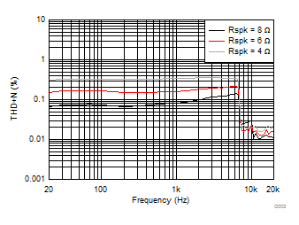
| PO = 1 W | VPVDD = 15 V |

| PO = 1 W | VPVDD = 24 V |

| Input Signal = 1 kHz | VPVDD = 15 V |

| Input Signal = 1 kHz | VPVDD = 24 V |

| RL = 8 Ω |

| LPVDD = 158 µA | DVDD = 3.3 V | |
| PDN = 0 |
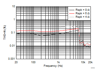
| PO = 1 W | VPVDD = 12 V |

| PO = 1 W | VPVDD = 18 V |
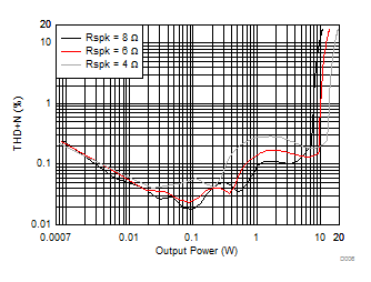
| f = 1 kHz | VPVDD = 12 V |

| Input Signal = 1 kHz | VPVDD = 16 V |

| RL = 8 Ω |

| RL = 8 Ω |
6.14.2 Typical Characteristics – PBTL Mode
.gif)
| THD+N = 10% |
.gif)
| PO = 1 W | VPVDD = 15 V |
.gif)
| PO = 1 W | VPVDD = 24 V |
.gif)
| f = 1 kHz | VPVDD = 15 V |
.gif)
| f = 1 kHz | Input Signal = 1 kHz Sine | VPVDD = 24 V |
.gif)
| RL = 8 Ω |
.gif)
| IPVDD = 159 µA | DVDD = 3.3 V | |
| PDN = 0 |
.gif)
| PO = 1 W | VPVDD = 12 V |
.gif)
| PO = 1 W | VPVDD = 18 V |
.gif)
| f = 1 kHz | VPVDD = 12 V |
.gif)
| f = 1 kHz | Input Signal = 1 kHz Sine | VPVDD = 18 V |
.gif)
| RL = 8 Ω |
.gif)
| RL = 8 Ω |
6.14.3 Typical Characteristics – Headphone Amplifier

| DRVDD = 3.3 V | PO = 10 mW | TA = 25 ºC |

| DRVDD = 3.3 V | VO = 1 Vrms | RL = 16 Ω |
| TA = 25 ºC |

| DRVDD = 3.3 V | f = 1 kHz | TA = 25 ºC |

| DRVDD = 3.3 V | VO = 1 Vrms | RL = 32 Ω |
| TA = 25 ºC |
6.14.4 Typical Characteristics – Line Driver

| DRVDD = 3.3 V | PO = 10 mW | TA = 25 ºC |
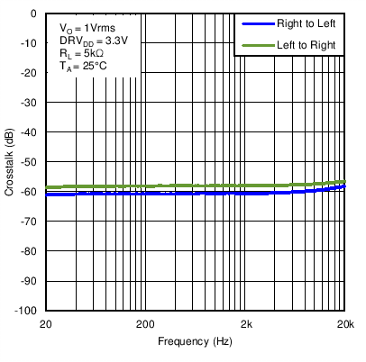
| DRVDD = 3.3 V | VO = 1 Vrms | RL = 5 kΩ |
| TA = 25 ºC |
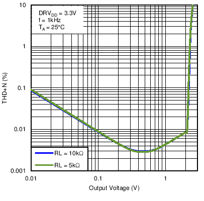
| DRVDD = 3.3 V | f = 1 kHz | TA = 25 ºC |