-
TFP410 TI PanelBus™ Digital Transmitter
- 1
- 1 Features
- 2 Applications
- 3 Description
- 4 Pin Configuration and Functions
- 5 Specifications
-
6 Detailed Description
- 6.1 Overview
- 6.2 Functional Block Diagram
- 6.3 Feature Description
- 6.4 Device Functional Modes
- 6.5 Programming
- 6.6
Register Maps
- 6.6.1 VEN_ID Register (Sub-Address = 01−00 ) [reset = 0x014C]
- 6.6.2 DEV_ID Register (Sub-Address = 03–02) [reset = 0x0410]
- 6.6.3 REV_ID Register (Sub-Address = 04) [reset = 0x00]
- 6.6.4 Reserved Register (Sub-Address = 07–05) [reset = 0x641400]
- 6.6.5 CTL_1_MODE (Sub-Address = 08) [reset = 0xBE]
- 6.6.6 CTL_2_MODE Register (Sub-Address = 09) [reset = 0x00]
- 6.6.7 CTL_3_MODE Register (Sub-Address = 0A) [reset = 0x80]
- 6.6.8 CFG Register (Sub-Address = 0B)
- 6.6.9 RESERVED Register (Sub-Address = 0E–0C) [reset = 0x97D0A9]
- 6.6.10 DE_DLY Register (Sub-Address = 32) [reset = 0x00]
- 6.6.11 DE_CTL Register (Sub-Address = 33) [reset = 0x00]
- 6.6.12 DE_TOP Register (Sub-Address = 34) [reset = 0x00]
- 6.6.13 DE_CNT Register (Sub-Address = 37–36) [reset = 0x0000]
- 6.6.14 DE_LIN Register (Sub-Address = 39–38) [reset = 0x0000]
- 6.6.15 H_RES Register (Sub-Address = 3B−3A)
- 6.6.16 V_RES Register (Sub-Address = 3D−3C)
- 7 Application and Implementation
- 8 Device and Documentation Support
- 9 Revision History
- 10Mechanical, Packaging, and Orderable Information
- IMPORTANT NOTICE
Package Options
Refer to the PDF data sheet for device specific package drawings
Mechanical Data (Package|Pins)
- PAP|64
Thermal pad, mechanical data (Package|Pins)
- PAP|64
Orderable Information
TFP410 TI PanelBus™ Digital Transmitter
1 Features
- Digital visual interface (DVI) compliant1
- Supports pixel rates up to 165MHz (including 1080p and WUXGA at 60Hz)
- Universal graphics controller interface:
- 12-bit, dual-edge and 24-bit, single-edge input modes
- Adjustable 1.1V to 1.8V and standard 3.3V CMOS input signal Levels
- Fully differential and single-ended input clocking modes
- Standard Intel 12-bit digital video port compatible as on Intel™ 81x Chipsets
- Enhanced PLL noise immunity:
- On-chip regulators and bypass capacitors for reducing system Costs
- Enhanced jitter performance:
- No HSYNC jitter anomaly
- Negligible data-dependent jitter
- Programmable using I2C serial interface
- Monitor detection through hot-plug and receiver detection
- Single 3.3V supply operation
- 64-Pin TQFP using TI’s PowerPAD™ package
- TI’s advanced 0.18µm EPIC-5™ CMOS process technology
- Pin compatible with SiI164 DVI transmitter(1)
3 Description
The TFP410 device is a Texas Instruments PanelBus™ flat-panel display product, part of a comprehensive family of end-to-end DVI 1.0-compliant solutions, targeted at the PC and consumer electronics industry.
The TFP410 device provides a universal interface to allow a glueless connection to most commonly available graphics controllers. Some of the advantages of this universal interface include selectable bus widths, adjustable signal levels, and differential and single-ended clocking. The adjustable 1.1V to 1.8V digital interface provides a low-EMI, high-speed bus that connects seamlessly with 12-bit or 24-bit interfaces. The DVI interface supports flat-panel display resolutions up to UXGA at 165MHz in 24-bit true color pixel format.
The TFP410 device combines PanelBus circuit innovation with TI’s advanced 0.18μm EPIC-5 CMOS process technology and TI’s ultra-low ground inductance PowerPAD package. The result is a compact 64-pin TQFP package providing a reliable, low-current, low-noise, high-speed digital interface solution.
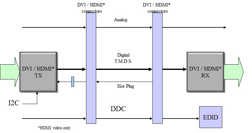
 Typical HDMI Interface