-
TL317 100-mA 3-Terminal Adjustable Positive Voltage Regulator
- 1 Features
- 2 Applications
- 3 Description
- 4 Revision History
- 5 Pin Configuration and Functions
- 6 Specifications
- 7 Detailed Description
-
8 Application and Implementation
- 8.1 Application Information
- 8.2
Typical Applications
- 8.2.1 Adjustable Voltage Regulator
- 8.2.2 0-V to 30-V Regulator Circuit
- 8.2.3 Regulator Circuit With Improved Ripple Rejection
- 8.2.4 Precision Current-Limiter Circuit
- 8.2.5 Tracking Preregulator Circuit
- 8.2.6 Slow-Turnon 15-V Regulator Circuit
- 8.2.7 50-mA Constant-Current Battery-Charger Circuit
- 8.2.8 Current-Limited 6-V Charger
- 8.2.9 High-Current Adjustable Regulator
- 9 Power Supply Recommendations
- 10Layout
- 11Device and Documentation Support
- 12Mechanical, Packaging, and Orderable Information
- IMPORTANT NOTICE
Package Options
Mechanical Data (Package|Pins)
Thermal pad, mechanical data (Package|Pins)
- PS|8
Orderable Information
TL317 100-mA 3-Terminal Adjustable Positive Voltage Regulator
1 Features
2 Applications
- Power Supplies
- Portable Devices
- Computing and Servers
- Telecommunications
- HVAC: Heating, Ventilation, and Air Conditioning
- Desktop PC
- Digital Signage
- Programmable Logic Controller
- Appliances
Functional Block Diagram

3 Description
The TL317 is an adjustable three-terminal positive-voltage regulator capable of supplying 100 mA over an output-voltage range of 1.25 V to 32 V. It is exceptionally easy to use and requires only two external resistors to set the output voltage.
This regulator offers full overload protection available only in integrated circuits. Included on the chip are current-limiting and thermal-overload protection. All overload-protection circuitry remains fully functional, even when ADJUSTMENT is disconnected. Normally, no capacitors are required unless the device is situated far from the input filter capacitors, in which case an input bypass is required. An optional output capacitor can be added to improve transient response. ADJUSTMENT can be bypassed to achieve very high ripple rejection.
In addition to replacing fixed regulators, the TL317 regulator is useful in a wide variety of other applications. Because the regulator is floating and sees only the input-to-output differential voltage, supplies of several hundred volts can be regulated as long as the maximum input-to-output differential is not exceeded. Its primary application is that of a programmable output regulator, but by connecting a fixed resistor between ADJUSTMENT and OUTPUT, this device can be used as a precision current regulator. Supplies with electronic shutdown can be achieved by clamping ADJUSTMENT to ground, programming the output to 1.25 V, where most loads draw little current.
Device Information(1)
| PART NUMBER | PACKAGE | BODY SIZE (NOM) |
|---|---|---|
| TL317D | SOIC (8) | 4.90 mm × 3.90 mm |
| TL317PW | TSSOP (8) | 4.30 mm × 3.00 mm |
| TL317PS | SOP (8) | 6.20 mm × 5.30 mm |
| TL317LP | TO-92 (3) | 4.83 mm × 3.68 mm |
- For all available packages, see the orderable addendum at the end of the data sheet.
4 Revision History
Changes from H Revision (September 2011) to I Revision
- Added ESD Ratings table, Feature Description section, Device Functional Modes, Application and Implementation section, Power Supply Recommendations section, Layout section, Device and Documentation Support section, and Mechanical, Packaging, and Orderable Information sectionGo
- Deleted Ordering Information table, see POA at the end of the datasheet.Go
Changes from G Revision (September 2009) to H Revision
5 Pin Configuration and Functions

6 Specifications
6.1 Absolute Maximum Ratings
over operating free-air temperature range (unless otherwise noted)(1)| MIN | MAX | UNIT | ||
|---|---|---|---|---|
| Input-to-output differential voltage, Vl – VO | 35 | V | ||
| Operating virtual-junction temperature, TJ | 150 | °C | ||
| Storage temperature range, Tstg | –65 | 150 | °C | |
6.2 ESD Ratings
| VALUE | UNIT | |||
|---|---|---|---|---|
| V(ESD) | Electrostatic discharge | Human-body model (HBM), per ANSI/ESDA/JEDEC JS-001(1) | ±2000 | V |
| Charged-device model (CDM), per JEDEC specification JESD22-C101(2) | ±1000(3) | |||
6.3 Recommended Operating Conditions
| MIN | NOM | MAX | UNIT | |||
|---|---|---|---|---|---|---|
| VI – VO | Input-to-output voltage differential | 2.5 | 35 | V | ||
| IO | Output current | 2.5 | 100 | mA | ||
| TJ | Operating virtual-junction temperature | TL317C | 0 | 125 | °C | |
| TL317 | –40 | 125 | °C | |||
6.4 Thermal Information
| THERMAL METRIC(1) | TL317 | UNIT | ||||
|---|---|---|---|---|---|---|
| D (SOIC) | PW (TSSOP) | PS (SOP) | LP (TO-92) | |||
| 8 PINS | 8 PINS | 8 PINS | 3 PINS | |||
| RθJA | Junction-to-ambient thermal resistance | 109.9 | 170 | 115.3 | 157.9 | °C/W |
| RθJC(top) | Junction-to-case (top) thermal resistance | 58.8 | 51 | 67.1 | 81.6 | °C/W |
| RθJB | Junction-to-board thermal resistance | 58.5 | 101.5 | 64.4 | — | °C/W |
| ψJT | Junction-to-top characterization parameter | 12.5 | 3.7 | 27.7 | 25.4 | °C/W |
| ψJB | Junction-to-board characterization parameter | 57.9 | 99.1 | 63.5 | 137.1 | °C/W |
6.5 Electrical Characteristics
over recommended operating virtual-junction temperature range (unless otherwise noted)(1)| PARAMETER | TEST CONDITIONS | MIN | TYP | MAX | UNIT | |
|---|---|---|---|---|---|---|
| Input voltage regulation(2) | VI – VO = 5 V to 35 V | TJ = 25°C | 0.01% | 0.02% | V | |
| IO = 2.5 mA to 100 mA | 0.02% | 0.05% | ||||
| Ripple regulation | VO = 10 V, f = 120 Hz | 65 | dB | |||
| VO = 10 V, 10-µF capacitor between ADJUSTMENT and ground |
66 | 80 | ||||
| Output voltage regulation | VI = 5 V to 35 V, IO = 2.5 mA to 100 mA, TJ = 25°C |
VO ≤ 5 V | 25 | mV | ||
| VO ≥ 5 V | 5 | mV/V | ||||
| VI = 5 V to 35 V, IO = 2.5 mA to 100 mA |
VO ≤ 5 | 50 | mV | |||
| VO ≥ 5 V | 10 | mV/V | ||||
| Output voltage change with temperature | TJ = 0°C to 125°C | 10 | mV/V | |||
| Output voltage long-term drift | After 1000 hours at TJ = 125°C and VI – VO = 35 V | 3 | 10 | mV/V | ||
| Output noise voltage | f = 10 Hz to 10 kHz, TJ = 25°C | 30 | µV/V | |||
| Minimum output current to maintain regulation | VI – VO = 35 | 1.5 | 2.5 | mA | ||
| Peak output current | VI – VO ≤ 35 V | 100 | 200 | mA | ||
| ADJUSTMENT current | 50 | 100 | µA | |||
| Change in ADJUSTMENT current | VI – VO = 2.5 V to 35 V, IO = 2.5 mA to 100 mA | 0.2 | 5 | µA | ||
| Reference voltage (output to ADJUSTMENT) |
IO = 2.5 mA to 100 mA, VI − VO = 5 V to 35 V, P ≤ rated dissipation |
1.2 | 1.25 | 1.3 | V | |
6.6 Typical Characteristic
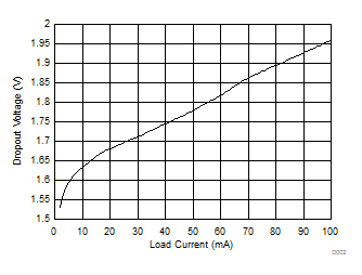 Figure 1. Dropout Voltage vs Load Current (TJ = 25°C)
7 Detailed Description
7.1 Overview
The TL317 device is an adjustable three-terminal positive-voltage regulator capable of supplying up to 100 mA over an output-voltage range of 1.25 V to 32 V. It requires only two external resistors to set the output voltage. The TL317 device is versatile in its applications, including uses in programmable output regulation and local on-card regulation. Also, by connecting a fixed resistor between the ADJUSTMENT and OUTPUT terminals, the TL317 device can function as a precision current regulator. An optional output capacitor can be added to improve transient response. The ADJUSTMENT terminal can be bypassed to achieve very high ripple-rejection ratios, which are difficult to achieve with standard three-terminal regulators.
7.2 Functional Block Diagrams
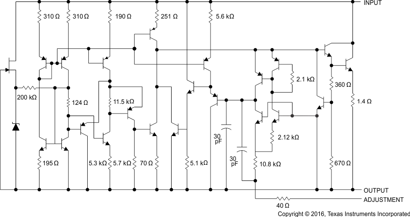
 Figure 2. Equivalent Schematic
7.3 Feature Description
7.3.1 NPN Darlington Output Drive
NPN Darlington output topology provides naturally low output impedance and an output capacitor is optional.
7.3.2 Programmable Feedback
An internal amplifier with 1.25-V offset input at the ADJUSTMENT terminal provides easy output voltage or current (not both) programming. For current regulation applications, a single resistor whose resistance value is 1.25 V / IO and power rating is greater than (1.25 V)2 / R must be used. For voltage regulation applications, two resistors set the output voltage as described in Adjustable Voltage Regulator.
7.4 Device Functional Modes
7.4.1 Normal Operation
The device OUTPUT pin sources current necessary to make the OUTPUT pin 1.25 V greater than the ADJUSTMENT pin to provide output regulation
7.4.2 Operation With Low Input Voltage
The device requires 2.5 V of headroom (VI – VO) to regulate the OUTPUT. With less headroom, the OUTPUT voltage of the device may be below the desired setpoint.
7.4.3 Operation in Light Loads
The device passes its bias current to the OUTPUT pin. The load or feedback must consume this minimum current for regulation or the output may be too high. The minimum current require to regulate is provided in the Electrical Characteristics, so the series resistance used to set the output voltage is recommended to be VO / IMIN to ensure regulation at all times.
8 Application and Implementation
NOTE
Information in the following applications sections is not part of the TI component specification, and TI does not warrant its accuracy or completeness. TI’s customers are responsible for determining suitability of components for their purposes. Customers should validate and test their design implementation to confirm system functionality.
8.1 Application Information
The flexibility of the TL317 allows it to be configured to take on many different functions in DC power applications.
8.2 Typical Applications
8.2.1 Adjustable Voltage Regulator
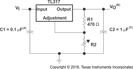 Figure 4. Adjustable Voltage Regulator
8.2.1.1 Design Requirements
- R1 and R2 are required to set the output voltage.
- C1 is recommended, particularly if the regulator is not in close proximity to the power-supply filter capacitors. A 0.1-µF ceramic or 1-µF tantalum capacitor provides sufficient bypassing for most applications, especially when adjustment and output capacitors are used.
- Use of an output capacitor, C2, improves transient response, but is optional.
8.2.1.2 Detailed Design Procedure
VO is calculated as shown in Equation 1. IADJ is typically 50 µA and negligible in most applications.
Power dissipation for linear regulators is calculated as shown in Equation 2. IADJ is typically 50 µA and negligible in most applications, so a typical way to calculate power dissipation for linear regulators is simplified to Equation 3.
8.2.1.3 Application Curve
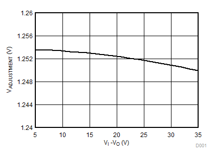 Figure 5. Line Regulation
8.2.2 0-V to 30-V Regulator Circuit
VO is calculated as shown in Equation 4, where Vref equals the difference between OUTPUT and ADJUSTMENT voltages (approximately 1.25 V).

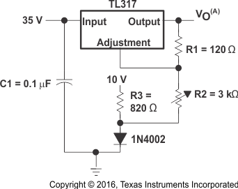 Figure 6. 0-V to 30-V Regulator Circuit Schematic
8.2.3 Regulator Circuit With Improved Ripple Rejection
- Protection diode D1 is recommended if C2 is used. The diode provides a low-impedance discharge path to prevent the capacitor from discharging into the output of the regulator
- Use of an output capacitor, C2, improves transient response, but is optional.
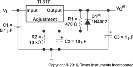 Figure 7. Regulator Circuit With Improved Ripple Rejection Schematic
8.2.4 Precision Current-Limiter Circuit
The use of the TL317 in this configuration limits the output current to Ilimit shown in Figure 8.
 Figure 8. Precision Current-Limiter Circuit
8.2.5 Tracking Preregulator Circuit
This application keeps a constant voltage across the second TL317 in the circuit.
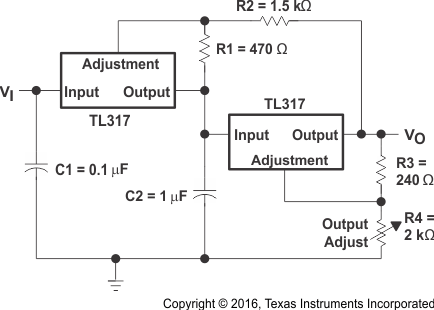 Figure 9. Tracking Preregulator Circuit Schematic
8.2.6 Slow-Turnon 15-V Regulator Circuit
The capacitor C1, in combination with the PNP transistor, helps the circuit to slowly start supplying voltage. In the beginning, the capacitor is not charged. Therefore, output voltage starts at VC1+ VBE + 1.25 V = 0 V + 0.65 V + 1.25 V = 1.9 V. As the capacitor voltage rises, VOUT also rises at the same rate. When the output voltage reaches the value determined by R1 and R2, the PNP is turned off.
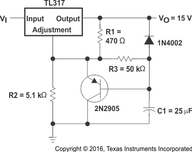 Figure 10. Slow-Turnon 15-V Regulator Circuit Schematic
8.2.7 50-mA Constant-Current Battery-Charger Circuit
The current limit operation mode can be used to trickle charge a battery at a fixed current. ICHG = 1.25 V / 24 Ω. VI must be greater than VBAT + 4.25 V (1.25 V [VREF] + 3 V [headroom]).
Power dissipation through resistor R1 is calculated as shown in Equation 5, so a resistor with the appropriate power rating must be chosen for this application.
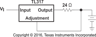 Figure 11. 50-mA Constant-Current Battery-Charger Circuit
8.2.8 Current-Limited 6-V Charger
As the charge current increases, the voltage at the bottom resistor increases until the NPN starts sinking current from the adjustment pin. The voltage at the adjustment pin drops, and consequently the output voltage decreases until the NPN stops conducting.
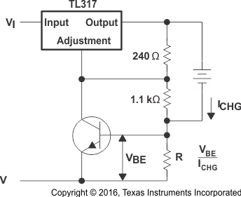 Figure 12. Current-Limited 6-V Charger Schematic
8.2.9 High-Current Adjustable Regulator
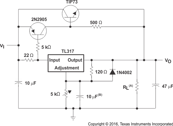
The NPNs at the top of the schematic allow higher currents at VOUT than the LM317 can provide, while still keeping the output voltage at levels determined by the adjustment pin resistor divider of the LM317.
