SCLS711A March 2009 – November 2015 TLC59210
PRODUCTION DATA.
- 1 Features
- 2 Applications
- 3 Description
- 4 Revision History
- 5 Pin Configuration and Functions
-
6 Specifications
- 6.1 Absolute Maximum Ratings
- 6.2 ESD Ratings
- 6.3 Recommended Operating Conditions
- 6.4 Thermal Information
- 6.5 Electrical Characteristics: VCC = 4.5 V to 5.5 V
- 6.6 Electrical Characteristics: VCC = 3 V to 3.6 V
- 6.7 Timing Requirements: VCC = 4.5 V to 5.5 V
- 6.8 Timing Requirements: VCC = 3 V to 3.6 V
- 6.9 Switching Characteristics: VCC = 4.5 V to 5.5 V
- 6.10 Switching Characteristics: VCC = 3 V to 3.6 V
- 6.11 Typical Characteristics
- 7 Parameter Measurement Information
- 8 Detailed Description
- 9 Application and Implementation
- 10Power Supply Recommendations
- 11Layout
- 12Device and Documentation Support
- 13Mechanical, Packaging, and Orderable Information
Package Options
Mechanical Data (Package|Pins)
Thermal pad, mechanical data (Package|Pins)
Orderable Information
1 Features
- DMOS Process
- High Voltage Output (Vds = 30 V)
- Output Current on Each Channel
(Ids Max = 200 mA) - Latch-Up Performance Exceeds 250 mA Per JEDEC Standard JESD-17
- ESD Protection Exceeds JESD 22
- 2000-V Human Body Model (A114-A)
- 200-V Machine Model (A115-A)
- 1000-V Charged Device Model (C101)
- LED Driver Application
- Output Clamp Diodes (Parasitic)
- Control Pins of CLR and CLK Inputs
- Clock Input up to 1 MHz
2 Applications
- Lamp and Display (LED)
- Hammer
- Relay
3 Description
The TLC59210 is an 8-bit flip-flop driver for LED and solenoid with Schmitt-trigger buffers. Each channel can sink up to 200mA and support an output voltage up to 30V. The TLC59210 is designed for VCC and operation from 3.3V to 5.5V.
Each output channel is controlled by a positive-edge-triggered D-type flip-flops with a direct clear (CLR) input. Information at the data (D) input meeting the setup time requirements is transferred to the Y output on the positive-going edge of the clock (CLK) pulse. Clock triggering occurs at a particular voltage level and is not directly related to the transition time of the positive-going pulse. When CLK is at either the high or low level, the D input has no effect at the output.
The TLC59210 is characterized for operation from –40°C to 85°C.
Device Information(1)
| PART NUMBER | PACKAGE | BODY SIZE (NOM) |
|---|---|---|
| TLC59210 | PDIP (20) | 24.33 mm × 6.35 mm |
| TSSOP (20) | 6.50 mm × 4.40 mm |
- For all available packages, see the orderable addendum at the end of the data sheet.
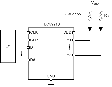
Typical Application Schematic
