TLC5958 48-Channel, 16-Bit ES-PWM LED Driver with Pre-Charge FET, LED Open Detection and Display Data Memory Support 32-Multiplexing
1 Features
- 48 Channels Constant Current Sink Output
- Sink Current Capability with Max BC/CC data:
- 25mA at 5VCC
- 20mA at 3.3VCC
- Global Brightness Control (BC) : 3-Bit (8 Step)
- Color Brightness Control (CC) for Each Color Group:
9-Bit (512 Step), Three Groups - Grayscale(GS) Control with Multiplexed Enhanced Spectrum(ES) PWM: 16bit
- 48K bit Grayscale Data Memory Support 32-multiplexing
- LED Power Supply Voltage Up To 10V
- Vcc = 3.0V to 5.5V
- Constant Current Accuracy
- Channel to Channel = ±1%(Typ), ±3%(Max)
- Device to Device = ±1%(Typ), ±2%(Max)
- Data Transfer Rate: 25MHz
- Gray Scale Clock: 33MHz
- LED Open Detection (LOD)
- Thermal Shut Down (TSD)
- IREF Resistor Short Protection (ISP)
- Power-Save Mode (PSM) with high speed recovery
- Delay Switching to Prevent Inrush Current
- Pre-charge FET to Avoid Ghosting Phenomenon
- Operating Temperature : –40°C to +85°C
2 Applications
- LED Video Displays with Multiplexing System
- LED Signboards with Multiplexing system
- High Refresh Rate & High density LED Panel
3 Description
The TLC5958 is a 48 channels constant-current sink driver for multiplexing system with 1 to 32 duty ratio. Each channel has an individually-adjustable, 65536-step, pulse width modulation (PWM) grayscale (GS).
48K bit display memory is implemented to increase the visual refresh rate and to decrease the GS data writing frequency.
The output channels are grouped into three groups, each group has 16 channels. Each group has a 512-step color brightness control (CC) function. The maximum current value of all 48 channels can be set by 8-step global brightness control (BC) function. CC and BC can be used to adjust the brightness deviation between LED drivers. GS, CC, and BC data are accessible via a serial interface port.
Send request via email for Application Note: Build High Density, High Refresh Rate, Multiplexing LED Panel with TLC5958.
Device Information(1)
| PART NUMBER | PACKAGE | BODY SIZE (NOM) |
|---|---|---|
| TLC5958 | VQFN (56) | 8.00 mm × 8.00 mm |
- For all available packages, see the orderable addendum at the end of the datasheet.
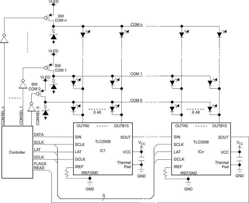
4 Typical Application Circuit (Multiple Daisy-Chained TLC5958s)
5 Revision History
Changes from * Revision (May 2014) to A Revision
- Deleted Product Preview banner - set to Production Data; global change Go
6 Description (Continued)
The TLC5958 has one error flag: LED open detection (LOD), which can be read via a serial interface port. The TLC5958 also has a power-save mode that sets the total current consumption to 0.8mA (typ) when all outputs are off.
7 Pin Configuration and Functions

Pin Functions
| PIN | I/O | DESCRIPTION | |
|---|---|---|---|
| NAME | NO. | ||
| GCLK | 29 | I | Grayscale(GS) pulse width modulation (PWM) reference clock control for OUTXn. Each GCLK rising edge increase the GS counter by1 for PWM control. |
| GND | ThermalPad | – | Power ground. The thermal pad must be soldered to GND on PCB. |
| IREF | 1 | – | Maximum constant-current value setting. The OUTR0 to OUTB15 maximum constant output current are set to the desired values by connecting an external resistor between IREF and IREFGND. See equation 1 for more detail. The external resistor should be placed close to the device. |
| IREFGND | 56 | – | Analog ground. Dedicated ground pin for the external IREF resistor. This pin should be connected to analog ground trace which is connected to power ground near the common GND point of board. |
| LAT | 27 | I | The LAT falling edge latches the data from the common shift register into the GS data memory or Function control(FC) register FC1 or FC2. |
| OUTR0-R15 | 8, 11, 14, 17, 20, 23, 30, 33, 36, 39, 44, 47, 50, 53 ,2, 5 | O | Constant current output for RED LED. Multiple outputs can be tied together to increase the constant current capability. Different voltages can be applied to each output. These outputs are turned on-off by GCLK signal and the data in GS data memory. |
| OUTG0-G15 | 9, 12, 15, 18, 21, 24, 31, 34, 37, 40, 45, 48, 51, 54, 3, 6 | O | Constant current output for GREEN LED. Multiple outputs can be tied together to increase the constant current capability. Different voltages can be applied to each output. These outputs are turned on-off by GCLK signal and the data in GS data memory. |
| OUTB0-B15 | 10, 13, 16, 19, 22, 25, 32, 35, 38, 41, 46, 49, 52, 55, 4, 7 | O | Constant current output for BLUE LED. Multiple outputs can be tied together to increase the constant current capability. Different voltages can be applied to each output. These outputs are turned on-off by GCLK signal and the data in GS data memory. |
| SCLK | 28 | I | Serial data shift clock. Data present on SIN are shifted to the 48-bit common shift register LSB with the SCLK rising edge. Data in the shift register are shifted towards the MSB at each SCLK rising edge. The common shift register MSB appears on SOUT. |
| SIN | 26 | I | Serial data input of the 48-bit common shift register. When SIN is high level, the LSB is set to '1' for only one SCLK input rising edge. If two SCLK rising edges are input while SIN is high, then the 48-bit shift register LSB and LSB+1 are set to '1'. When SIN is low, the LSB is set to '0' at the SCLK input rising edge. |
| SOUT | 42 | O | Serial data output of the 48-bit common shift register. SOUT is connected to the MSB of the register. |
| VCC | 43 | – | Power-supply voltage. |