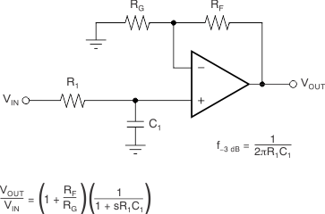
The TLV316 (single), TLV2316 (dual), and TLV4316 (quad) devices comprise a family of general-purpose, low-power operational amplifiers. Features such as rail-to-rail input and output swings, low quiescent current (400 μA/ch typical) combined with a wide bandwidth of 10 MHz, and very-low noise (12 nV/√Hz at 1 kHz) make this family attractive for a variety of applications that require a good balance between cost and performance. The low input bias current supports operational amplifiers that are used in applications with megaohm source impedances.
The robust design of the TLVx316 provides ease-of-use to the circuit designer—a unity-gain stable, integrated RFI/EMI rejection filter, no phase reversal in overdrive condition, and high electrostatic discharge (ESD) protection (4-kV HBM).
These devices are optimized for low-voltage operation as low as 1.8 V (±0.9 V) and up to 5.5 V (±2.75 V). This latest addition of low-voltage CMOS operational amplifiers to the portfolio, in conjunction with the TLVx313 and TLVx314 series, offer a family of bandwidth, noise, and power options to meet the needs of a wide variety of applications.
PART NUMBER | PACKAGE | BODY SIZE (NOM) |
---|---|---|
TLV316 | SC70 (5) | 1.25 mm × 2.00 mm |
SOT-23 (5) | 1.60 mm × 2.90 mm | |
TLV2316 | VSSOP (8) | 3.00 mm × 3.00 mm |
SOIC (8) | 3.91 mm × 4.90 mm | |
TLV4316 | TSSOP (14) | 4.40 mm × 5.00 mm |
SOIC (14) | 8.65 mm × 3.91 mm |
PIN | I/O | DESCRIPTION | ||
---|---|---|---|---|
NAME | DBV (SOT-23) | DCK (SC70) | ||
–IN | 4 | 3 | I | Inverting input |
+IN | 3 | 1 | I | Noninverting input |
OUT | 1 | 4 | O | Output |
V– | 2 | 2 | — | Negative (lowest) supply or ground (for single-supply operation) |
V+ | 5 | 5 | — | Positive (highest) supply |
PIN | I/O | DESCRIPTION | |
---|---|---|---|
NO. | NAME | ||
2 | –IN A | I | Inverting input, channel A |
3 | +IN A | I | Noninverting input, channel A |
6 | –IN B | I | Inverting input, channel B |
5 | +IN B | I | Noninverting input, channel B |
1 | OUT A | O | Output, channel A |
7 | OUT B | O | Output, channel B |
4 | V– | — | Negative (lowest) supply or ground (for single-supply operation) |
8 | V+ | — | Positive (highest) supply |
PIN | I/O | DESCRIPTION | |
---|---|---|---|
NO. | NAME | ||
2 | –IN A | I | Inverting input, channel A |
3 | +IN A | I | Noninverting input, channel A |
6 | –IN B | I | Inverting input, channel B |
5 | +IN B | I | Noninverting input, channel B |
9 | –IN C | I | Inverting input, channel C |
10 | +IN C | I | Noninverting input, channel C |
13 | –IN D | I | Inverting input, channel D |
12 | +IN D | I | Noninverting input, channel D |
1 | OUT A | O | Output, channel A |
7 | OUT B | O | Output, channel B |
8 | OUT C | O | Output, channel C |
14 | OUT D | O | Output, channel D |
11 | V– | — | Negative (lowest) supply or ground (for single-supply operation) |
4 | V+ | — | Positive (highest) supply |
MIN | MAX | UNIT | |||
---|---|---|---|---|---|
Supply voltage | 7 | V | |||
Signal input pins | Voltage(2) | Common-mode | (V–) – 0.5 | (V+) + 0.5 | V |
Differential | (V+) – (V–) + 0.2 | ||||
Current(2) | –10 | 10 | mA | ||
Output short-circuit(3) | Continuous | mA | |||
Temperature | Specified, TA | –40 | 125 | °C | |
Junction, TJ | 150 | ||||
Storage, Tstg | –65 | 150 |
VALUE | UNIT | |||
---|---|---|---|---|
V(ESD) | Electrostatic discharge | Human body model (HBM), per ANSI/ESDA/JEDEC JS-001(1) | ±4000 | V |
Charged device model (CDM), per JEDEC specification JESD22-C101(2) | ±1500 |
MIN | NOM | MAX | UNIT | |||
---|---|---|---|---|---|---|
VS | Supply voltage | 1.8 | 5.5 | V | ||
Specified temperature range | –40 | 125 | °C |
THERMAL METRIC(1) | TLV316 | UNIT | ||
---|---|---|---|---|
DBV (SOT-23) | DCK (SC70) | |||
5 PINS | 5 PINS | |||
RθJA | Junction-to-ambient thermal resistance | 221.7 | 263.3 | °C/W |
RθJC(top) | Junction-to-case(top) thermal resistance | 144.7 | 75.5 | °C/W |
RθJB | Junction-to-board thermal resistance | 49.7 | 51.0 | °C/W |
ψJT | Junction-to-top characterization parameter | 26.1 | 1.0 | °C/W |
ψJB | Junction-to-board characterization parameter | 49.0 | 50.3 | °C/W |
RθJC(bot) | Junction-to-case(bottom) thermal resistance | N/A | N/A | °C/W |
THERMAL METRIC(1) | TLV2316 | UNIT | ||
---|---|---|---|---|
D (SOIC) | DGK (VSSOP) | |||
8 PINS | 8 PINS | |||
RθJA | Junction-to-ambient thermal resistance | 127.2 | 186.6 | °C/W |
RθJC(top) | Junction-to-case(top) thermal resistance | 71.6 | 78.8 | °C/W |
RθJB | Junction-to-board thermal resistance | 68.2 | 107.9 | °C/W |
ψJT | Junction-to-top characterization parameter | 22.0 | 15.5 | °C/W |
ψJB | Junction-to-board characterization parameter | 67.6 | 106.3 | °C/W |
RθJC(bot) | Junction-to-case(bottom) thermal resistance | N/A | N/A | °C/W |
THERMAL METRIC(1) | TLV4316 | UNIT | ||
---|---|---|---|---|
PW (TSSOP) | D (SOIC) | |||
14 PINS | 14 PINS | |||
RθJA | Junction-to-ambient thermal resistance | 117.2 | 87.0 | °C/W |
RθJC(top) | Junction-to-case(top) thermal resistance | 46.2 | 44.4 | °C/W |
RθJB | Junction-to-board thermal resistance | 58.9 | 41.7 | °C/W |
ψJT | Junction-to-top characterization parameter | 4.9 | 11.6 | °C/W |
ψJB | Junction-to-board characterization parameter | 58.3 | 41.4 | °C/W |
RθJC(bot) | Junction-to-case(bottom) thermal resistance | N/A | N/A | °C/W |
PARAMETER | TEST CONDITIONS | MIN | TYP | MAX | UNIT | ||
---|---|---|---|---|---|---|---|
OFFSET VOLTAGE | |||||||
VOS | Input offset voltage | VS = 5 V | ±0.75 | ±3 | mV | ||
VS = 5 V, TA = –40°C to +125°C | ±4.5 | ||||||
dVOS/dT | Drift | VS = 5 V, TA = –40°C to +125°C | ±2 | µV/°C | |||
PSRR | Power-supply rejection ratio | VS = 1.8 V – 5.5 V, VCM = (V–) | ±30 | ±175 | µV/V | ||
Channel separation, dc | At dc | 100 | dB | ||||
INPUT VOLTAGE RANGE | |||||||
VCM | Common-mode voltage range | VS = 5.5 V | (V–) – 0.2 | (V+) + 0.2 | V | ||
CMRR | Common-mode rejection ratio | VS = 5.5 V, (V–) – 0.2 V < VCM < (V+) – 1.4 V, TA = –40°C to +125°C |
72 | 90 | dB | ||
VS = 5.5 V, VCM = –0.2 V to 5.7 V, TA = –40°C to +125°C |
75 | ||||||
INPUT BIAS CURRENT | |||||||
IB | Input bias current | ±10 | pA | ||||
IOS | Input offset current | ±10 | pA | ||||
NOISE | |||||||
En | Input voltage noise (peak-to-peak) | VS = 5 V, f = 0.1 Hz to 10 Hz | 5 | µVPP | |||
en | Input voltage noise density | VS = 5 V, f = 1 kHz | 12 | nV/√Hz | |||
in | Input current noise density | f = 1 kHz | 1.3 | fA/√Hz | |||
INPUT IMPEDANCE | |||||||
ZID | Differential | 2 || 2 | 1016Ω || pF | ||||
ZIC | Common-mode | 2 || 4 | 1011Ω || pF | ||||
OPEN-LOOP GAIN | |||||||
AOL | Open-loop voltage gain | VS = 5.5 V, (V–) + 0.05 V < VO < (V+) – 0.05 V, RL = 10 kΩ |
100 | 104 | dB | ||
VS = 5.5 V, (V–) + 0.15 V < VO < (V+) – 0.15 V, RL = 2 kΩ |
104 | ||||||
FREQUENCY RESPONSE | |||||||
GBP | Gain bandwidth product | VS = 5 V, G = +1 | 10 | MHz | |||
φm | Phase margin | VS = 5 V, G = +1 | 60 | Degrees | |||
SR | Slew rate | VS = 5 V, G = +1 | 6 | V/μs | |||
tS | Settling time | To 0.1%, VS = 5 V, 2-V step , G = +1, CL = 100 pF | 1 | μs | |||
tOR | Overload recovery time | VS = 5 V, VIN × gain = VS | 0.8 | μs | |||
THD + N | Total harmonic distortion + noise(1) | VS = 5 V, VO = 0.5 VRMS, G = +1, f = 1 kHz | 0.008% | ||||
OUTPUT | |||||||
VO | Voltage output swing from supply rails | VS = 1.8 V to 5.5 V, RL = 10 kΩ, | 35 | mV | |||
VS = 1.8 to 5.5 V, RL = 2 kΩ, | 125 | ||||||
ISC | Short-circuit current | VS = 5 V | ±50 | mA | |||
ZO | Open-loop output impedance | VS = 5 V, f = 10 MHz | 250 | Ω | |||
POWER SUPPLY | |||||||
VS | Specified voltage range | 1.8 | 5.5 | V | |||
IQ | Quiescent current per amplifier | VS = 5 V, IO = 0 mA, TA = –40°C to 125°C | 400 | 575 | µA | ||
TEMPERATURE | |||||||
TA | Specified | –40 | 125 | °C | |||
Tstg | Storage | –65 | 150 | °C |
TITLE | FIGURE |
---|---|
Offset Voltage Production Distribution | Figure 1 |
Offset Voltage vs Common-Mode Voltage | Figure 2 |
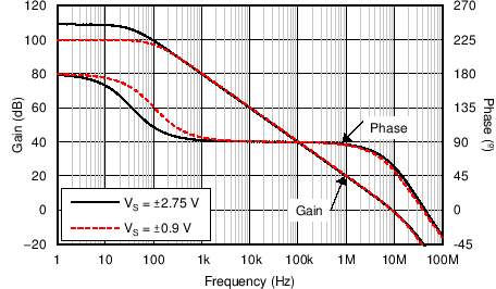
Open- Loop Gain and Phase vs Frequency | Figure 3 |
Input Bias and Offset Current vs Temperature | Figure 4 |
Input Voltage Noise Spectral Density vs Frequency | Figure 5 |
Quiescent Current vs Supply Voltage | Figure 6 |
Small-Signal Overshoot vs Load Capacitance | Figure 7 |
No Phase Reversal | Figure 8 |
Small-Signal Step Response | Figure 9 |
Large-Signal Step Response | Figure 10 |
Short-Circuit Current vs Temperature | Figure 11 |
Electromagnetic Interference Rejection Ratio Referred to Noninverting Input vs Frequency | Figure 12 |
Channel Separation vs Frequency | Figure 13 |
Distribution taken from 12551 amplifiers |
VCM < (V+) – 1.4 V | ||
V+ = 2.75 V, V– = –2.75 V, G = –1 V/V | ||
V+ = 2.75 V, V– = –2.75 V, G = 1 V/V | ||
V+ = 2.75 V, V– = –2.75 V | ||
V+ = 2.75 V, V– = –2.75 V, 9 typical units shown | ||
V+ = 2.75 V, V– = –2.75 V | ||
V+ = 2.75 V, V– = –2.75 V, CL = 100 pF, G = 1 V/V | ||
PRF = –10 dBm | ||