-
TLV705 200-mA, Low IQ, Low-Noise, Low-Dropout Regulator in Ultra-Small, 0.77-mm × 0.77-mm DSBGA and PicoStar
- 1 Features
- 2 Applications
- 3 Description
- 4 Revision History
- 5 Pin Configuration and Functions
- 6 Specifications
- 7 Detailed Description
- 8 Application and Implementation
- 9 Power Supply Recommendations
- 10Layout
- 11Device and Documentation Support
- 12Mechanical, Packaging, and Orderable Information
- IMPORTANT NOTICE
Package Options
Mechanical Data (Package|Pins)
Thermal pad, mechanical data (Package|Pins)
Orderable Information
TLV705 200-mA, Low IQ, Low-Noise, Low-Dropout Regulator in Ultra-Small, 0.77-mm × 0.77-mm DSBGA and PicoStar
1 Features
-
Very Low Dropout:
- 105 mV at IOUT = 150 mA
- 145 mV at IOUT = 200 mA
- Accuracy: 0.5% Typical
- Low IQ: 35 μA
- Available in Fixed-Output Voltages From
0.7 V to 4.8 V - VIN Range: 2 V to 5.5 V
- High PSRR: 70 dB at 1 kHz
- Stable With Effective Capacitance of 0.1 μF
- Thermal Shutdown and Overcurrent Protection
- Available in an Ultra-Low Profile (0.15-mm Maximum Height) PicoStar Package Option
2 Applications
3 Description
The TLV705 series of low-dropout (LDO) linear regulators are low quiescent current devices with excellent line and load transient performance. These devices are designed for power-sensitive applications, with a precision band gap. An error amplifier provides typical accuracy of 0.5%. Low output noise, very high power-supply rejection ratio (PSRR), and low dropout voltage make this series of LDOs ideal for a wide selection of battery-operated handheld equipment. All devices have a thermal shutdown and current limit for safety.
Furthermore, the TLV705 series is stable with an effective output capacitance of only 0.1 μF. This feature enables the use of cost-effective capacitors that have higher bias voltage and temperature derating. The devices regulate to the specified accuracy with zero output load. The TLV705P series also provides an active pulldown circuit to quickly discharge output.
The TLV705 and TLV705P series are both available in 0.77-mm × 0.77-mm DSBGA and PicoStar packages with three height options that are optimal for handheld applications.
Device Information(1)
| PART NUMBER | PACKAGE | BODY SIZE (NOM) |
|---|---|---|
| TLV705 | DSGBA (4) | 0.77 mm × 0.77 mm |
| PicoStar (4) | 0.77 mm × 0.77 mm |
- For all available packages, see the orderable addendum at the end of the data sheet.
4 Revision History
Changes from E Revision (May 2015) to F Revision
- Deleted "x" from TLV705 device in document title Go
- Changed package dimensions in document title from "0.8-mm × 0.8-mm" to "0.77-mm × 0.77-mm" Go
- Changed ultra-low profile maximum height from 0.2-mm to 0.15-mm in Applications section Go
- Changed package dimensions in Description section from 0.8-mm to 0.77-mm.Go
- Changed DSBGA package dimensions from "0.80 mm × 0.80 mm" to "0.77 mm × 0.77 mm" in the Device Information table Go
- Added copyright statement to the Typical Application Circuit Go
- Changed formatting of Thermal Information table note Go
- Deleted "x" from device number in Thermal Information table Go
- Added copyright statement to functional block diagrams in Functional Block Diagrams section Go
- Added copyright statement to Typical Application Circuit (Fixed-Voltage Versions) in the Typical Application section Go
- Changed formatting of document reference in Related Documentation section Go
- Changed table header title from "Sample & Buy" to "Order Now" in the Related Links table Go
Changes from D Revision (April 2015) to E Revision
- Added new package (YFM) to document Go
- Added PicoStar to title Go
- Changed last Features bullet Go
- Changed last sentence of Description section Go
- Added second row to Device Information table Go
- Added YFM pin out drawingGo
- Added YFM package to Thermal Information table Go
- Changed VO parameter units in Electrical Characteristics table: % for first row, mV for second rowGo
- Changed first sentence of Overview section: removed new Go
- Changed fifth sentence of Internal Current Limit section to clarify description of the shutdown circuit functionality Go
- Changed Vµs to V/µs in second paragraph of Start-Up Current section Go
- Changed it to the start-up current in third paragraph of Start-Up Current section Go
- Changed INPUT to VIN in Power Supply Recommendations section Go
- Added Related Links section Go
- Added YFM package to Package Mounting section Go
Changes from C Revision (October 2012) to D Revision
- Added ESD Ratings table, Feature Description section, Device Functional Modes, Application and Implementation section, Power Supply Recommendations section, Layout section, Device and Documentation Support section, and Mechanical, Packaging, and Orderable Information section Go
- Added Features bullet for VIN range Go
- Changed Applications list items Go
- Deleted Power Dissipation Ratings table Go
- Changed y-axis unit measurement from ILIM to ICL for Figure 11Go
- Changed Figure 31 and deleted layout silkscreen images; replaced with image of PCB layout drawing.Go
- Changed title for Figure 31 Go
- Changed title of Thermal Protection section Go
Changes from B Revision (December 2011) to C Revision
- Deleted last Features bulletGo
Changes from A Revision (August 2011) to B Revision
5 Pin Configuration and Functions
Pin Functions
| PIN | I/O | DESCRIPTION | |
|---|---|---|---|
| NAME | NO. | ||
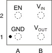
| GND | A1 | — | Ground pin. |
| EN | A2 | I | Enable pin. Driving EN over 0.9 V turns on the regulator. Driving EN below 0.4 V places the regulator into shutdown mode, which reduces the operating current to 1 μA (nominal). |
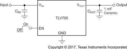
| VOUT | B1 | O | Regulated output voltage pin. Placing a small 1-μF ceramic capacitor is required from this pin to ground to ensure stability. See Input and Output Capacitor Requirements for more details. |
| VIN | B2 | I | Input pin. TI recommends placing a small 1-µF capacitor from this pin to ground for good transient performance. See Input and Output Capacitor Requirements for more details. |

