SBVS217B June 2013 – November 2015 TLV716P
PRODUCTION DATA.
- 1 Features
- 2 Applications
- 3 Description
- 4 Revision History
- 5 Pin Configuration and Functions
- 6 Specifications
- 7 Detailed Description
- 8 Application and Implementation
- 9 Power Supply Recommendations
- 10Layout
- 11Device and Documentation Support
- 12Mechanical, Packaging, and Orderable Information
Package Options
Mechanical Data (Package|Pins)
- DPQ|6
Thermal pad, mechanical data (Package|Pins)
- DPQ|6
Orderable Information
1 Features
2 Applications
- Wireless Handsets, Smart Phones, Tablets
- Set-Top Boxes (STBs), Cameras, Modems
- Portable Battery-Powered Products
3 Description
The TLV716 is a family of dual-channel, capacitor-free,150-mA, low-dropout (LDO) voltage regulators with multiple fixed-output options available from 1 V to 3.3 V. These devices provide an initial 1% accuracy and 1.5% accuracy overtemperature.
The TLV716 family is designed to be stable with or without an input or output capacitor. Eliminating the output capacitor allows for a very small solution size. The TLV716P series provides an active pulldown circuit to quickly discharge the output voltage if the application requires an output capacitor.
The device provides inrush current control during device power up and enabling. Inrush control provides constant-current charging of the output load during start-up, thereby reducing the risk of an undesired overcurrent fault from the input supply or battery.
The TLV716 family is available in a 1.2-mm × 1.2-mm SON-6 package and is ideal for space-constrained applications.
Device Information(1)
| PART NUMBER | PACKAGE | BODY SIZE (NOM) |
|---|---|---|
| TLV716 | X2SON (6) | 1.20 mm × 1.20 mm |
| TLV716P |
- For all available packages, see the orderable addendum at the end of the data sheet.
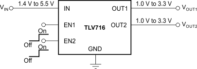
Typical Application Circuit
