SLLS907E August 2008 – August 2014 TPD4F003 , TPD6F003 , TPD8F003
PRODUCTION DATA.
- 1 Features
- 2 Applications
- 3 Description
- 4 Revision History
- 5 Pin Configuration and Functions
- 6 Specifications
-
7 Detailed Description
- 7.1 Overview
- 7.2 Functional Block Diagram
- 7.3
Feature Description
- 7.3.1 Four-, Six-, and Eight-Channel EMI Filtering for Data Ports
- 7.3.2 -3 dB Bandwidth of 200 MHz
- 7.3.3 Greater Than 25 dB Attenuation at 1 GHz
- 7.3.4 Robust ESD Protection Exceeds IEC 61000-4-2
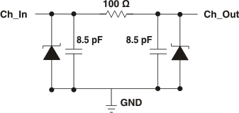
- 7.3.5 Pi-Style (C-R-C) Filter Configuration
- 7.3.6 Low 10-nA Leakage Current
- 7.3.7 Easy Flow-Through Routing
- 7.4 Device Functional Modes
- 8 Applications and Implementation
- 9 Power Supply Recommendations
- 10Layout
- 11Device and Documentation Support
- 12Mechanical, Packaging, and Orderable Information
Package Options
Refer to the PDF data sheet for device specific package drawings
Mechanical Data (Package|Pins)
- DQD|12
Thermal pad, mechanical data (Package|Pins)
- DQD|12
Orderable Information
1 Features
- Four-, Six-, and Eight-Channel EMI Filtering for Data Ports
- –3 dB Bandwidth of 200 MHz
- Greater than 25 dB attenuation at 1 GHz
- IEC 61000-4-2 Level 4 ESD Protection
- ±12-kV Contact Discharge
- ±20-kV Air Gap Discharge
- Pi-Style (C-R-C) Filter Configuration
(R = 100 Ω, CTOTAL = 17 pF) - Low 10-nA Leakage Current
- Easy Flow-Through Routing
2 Applications
- Display Interfaces
- Cell Phones
- Tablets
- SVGA Video Connections
- Memory Interfaces
3 Description
The TPDxF003 family is a series of highly integrated devices designed to provide Electromagnetic Interference (EMI) filtering in all systems subjected to electromagnetic interference. These filters also provide a Transient Voltage Suppressor (TVS) diode circuit for Electrostatic Discharge (ESD) protection which prevents damage to the application when subjected to ESD stress far exceeding IEC 61000-4-2 (Level 4).
The TPDxF003 family is specified for –40°C to 85°C operation. These filters are also packaged in space-saving 0.4-mm pitch DQD packages.
Device Information(1)
| PART NUMBER | PACKAGE | BODY SIZE (NOM) |
|---|---|---|
| TPD4F003 | WSON (8) | 1.70 mm x 1.35 mm |
| TPD6F003 | WSON (12) | 2.50 mm x 1.35 mm |
| TPD8F003 | WSON (16) | 3.30 mm x 1.35 mm |
- For all available packages, see the orderable addendum at the end of the datasheet.
Equivalent Schematic