-
TPS2378 IEEE 802.3at PoE High-Power PD Interface
- 1 Features
- 2 Applications
- 3 Description
- 4 Revision History
- 5 Pin Configuration and Functions
- 6 Specifications
-
7 Detailed Description
- 7.1 Overview
- 7.2 Functional Block Diagram
- 7.3 Feature Description
- 7.4
Device Functional Modes
- 7.4.1 PoE Overview
- 7.4.2 Threshold Voltages
- 7.4.3 PoE Start-up Sequence
- 7.4.4 Detection
- 7.4.5 Hardware Classification
- 7.4.6 Inrush and Start-up
- 7.4.7 Maintain Power Signature
- 7.4.8 Start-up and Converter Operation
- 7.4.9 PD Hotswap Operation
- 7.4.10 Start-up and Power Management, CDB and T2P
- 7.4.11 Adapter ORing
- 7.4.12 Using DEN to Disable PoE
- 7.4.13 ORing Challenges
- 8 Application and Implementation
- 9 Power Supply Recommendations
- 10Layout
- 11Device and Documentation Support
- 12Mechanical, Packaging, and Orderable Information
- IMPORTANT NOTICE
Package Options
Mechanical Data (Package|Pins)
- DDA|8
Thermal pad, mechanical data (Package|Pins)
- DDA|8
Orderable Information
DATA SHEET
TPS2378 IEEE 802.3at PoE High-Power PD Interface
1 Features
2 Applications
- IEEE 802.3at-compliant Devices
- Video and VoIP Telephones
- Multiband Access Points
- Security Cameras
- Pico-base Stations
- Forced, Four-Pair, High Power Devices (SLVA625)
3 Description
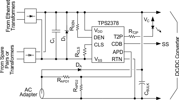
This 8-pin integrated circuit contains all of the features needed to implement an IEEE802.3at type-2 powered device (PD). The low 0.5-Ω internal switch resistance, combined with the enhanced thermal dissipation of the PowerPAD™ package, enables this controller to continuously handle up to 0.85 A. The TPS2378 features an auxiliary power detect (APD) input, providing priority for an external power adapter. It also features a 100-V pass transistor, 140-mA inrush current limiting, type-2 indication, auto-retry fault protection, and an open-drain power-good output.
Device Information(1)
| PART NUMBER | PACKAGE | BODY SIZE (NOM) |
|---|---|---|
| TPS2378 | HSOP (8) | 4.89 mm × 3.90 mm |
- For all available packages, see the orderable addendum at the end of the data sheet.
Typical Application Circuit

4 Revision History
Changes from B Revision (November 2012) to C Revision
- Added ESD Ratings table, Feature Description section, Device Functional Modes, Application and Implementation section, Power Supply Recommendations section, Layout section, Device and Documentation Support section, and Mechanical, Packaging, and Orderable Information section Go
- Deleted Detailed Pin Description section. Go
- Deleted CBD Pin Interface sectionGo
- Deleted APD Pin Divider Network, RAPD1, RAPD2 sectionGo
Changes from A Revision (March 2012) to B Revision
- Added Application: Forced, Four-Pair, High Power Devices (SLVA625)Go
- Added Note 1 to the ELECTRICAL CHARACTERISTICS tableGo
- Added section: Forced, Four-Pair, High Power PoE Go
- Changed Table 2, From: POWER ≤ 12.95W To: POWER ≤ 13W, From: POWER > 12.95W To POWER > 13W, and PD INPUT POWER (max) From: 12.95 W To 13W Go
- Changed Table 2, PSE Output Power for 802.3at (Type 2) From: 36W to 30WGo
- Changed text in the Detection section From: "( ΔV / ΔI ) between 23.75 kΩ and 26.25 kΩ at the PI." To: "( ΔV / ΔI ) between 23.7 kΩ and 26.3 kΩ at the PI." Go
- Added text to the Startup and Converter Operation section: "Additional loading applied between VVDD and VRTN during the inrush state may prevent successful PD and subsequent converter start up."Go
- Changed text in the Detection Resistor, RDEN section From: "RDEN between 23.75 kΩ and 26.25 kΩ, or 25 kΩ ± 5%. " To: "RDEN between 23.7 kΩ and 26.3 kΩ, or 25 kΩ ± 5%."Go
Changes from * Revision (March 2012) to A Revision
- Changed the Inrush termination MAX value From: 100% To: 99%Go
5 Pin Configuration and Functions
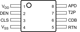
DDA Package
8-Pin HSOP
Top View

Pin Functions
| PIN | I/O | DESCRIPTION | |
|---|---|---|---|
| NAME | NO. | ||
| VDD | 1 | I | Connect to positive PoE input power rail. Bypass with 0.1 µF to VSS. |
| DEN | 2 | I/O | Connect 24.9 kΩ to VDD for detection. Pull to VSS disable pass MOSFET. |
| CLS | 3 | O | Connect resistor from CLS to VSS to program classification current. |
| VSS | 4 | — | Connect to negative power rail derived from PoE source. |
| RTN | 5 | — | Drain of PoE pass MOSFET. |
| CDB | 6 | O | Active low, open-drain converter disable output, referenced to RTN. |
| T2P | 7 | O | Active low indicates type 2 PSE connected or APD active. |
| APD | 8 | I | Raise 1.5 V above RTN to disable pass MOSFET and force T2P active. |
| Pad | — | — | The PowerPad™ must be connected to VSS. A large fill area is required to assist in heat dissipation. |