-
TPS25924x 12-V eFuse with Over Voltage Protection and Blocking FET Control
- 1 Features
- 2 Applications
- 3 Description
- 4 Revision History
- 5 Device Comparison Table
- 6 Pin Configuration and Functions
- 7 Specifications
- 8 Detailed Description
-
9 Application and Implementation
- 9.1 Application Information
- 9.2
Typical Applications
- 9.2.1
Simple 3.7-A eFuse Protection for Set Top Boxes
- 9.2.1.1 Design Requirements
- 9.2.1.2 Detailed Design Procedure
- 9.2.1.3 Application Curves
- 9.2.2 Inrush and Reverse Current Protection for Hold-Up Capacitor Application (for example, SSD)
- 9.2.3 Controlled Power Down using TPS25924x
- 9.2.1
Simple 3.7-A eFuse Protection for Set Top Boxes
- 10Power Supply Recommendations
- 11Layout
- 12Device and Documentation Support
- 13Mechanical, Packaging, and Orderable Information
- IMPORTANT NOTICE
Package Options
Mechanical Data (Package|Pins)
- DRC|10
Thermal pad, mechanical data (Package|Pins)
- DRC|10
Orderable Information
TPS25924x 12-V eFuse with Over Voltage Protection and Blocking FET Control
1 Features
- VOPERATING = 4.5 V to 13.8 V, VABSMAX = 20 V
- Integrated 28-mΩ Pass MOSFET
- Fixed 15-V Over Voltage Clamp
- 1-A to 5-A Adjustable ILIMIT
- ±8% ILIMIT Accuracy at 3.7 A
- Reverse Current Blocking Support
- Programmable OUT Slew Rate, UVLO
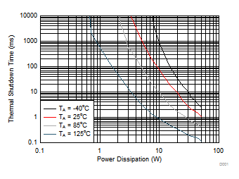
- Built-in Thermal Shutdown
- UL 2367 Recognized – File No. E339631*
- *RILIM ≤ 130 kΩ (5 A maximum)
- Safe During Single Point Failure Test (UL60950)
- Small Foot Print – 10L (3 mm x 3 mm) VSON
2 Applications
- Adapter Powered Devices
- HDD and SSD Drives
- Set Top Boxes
- Servers / AUX Supplies
- Fan Control
- PCI/PCIe Cards
3 Description
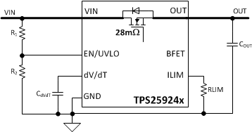
The TPS25924x family of eFuses is a highly integrated circuit protection and power management solution in a tiny package. The devices use few external components and provide multiple protection modes. They are a robust defense against overloads, shorts circuits, voltage surges, excessive inrush current, and reverse current.
Current limit level can be set with a single external resistor. Over voltage events are limited by internal clamping circuits to a safe fixed maximum, with no external components required.
Applications with particular voltage ramp requirements can set dV/dT with a single capacitor to ensure proper output ramp rates. Many systems, such as SSDs, must not allow holdup capacitance energy to dump back through the FET body diode onto a drooping or shorted input bus. The BFET pin is for such systems. An external NFET can be connected “Back to Back (B2B)” with the TPS25924x output and the gate driven by BFET to prevent current flow from load to source (see Figure 43).
Device Information(1)
| PART NUMBER | PACKAGE | BODY SIZE (NOM) |
|---|---|---|
| TPS259241 | VSON (10) | 3.00 mm × 3.00 mm |
| TPS259240 |
- For all available packages, see the orderable addendum at the end of the data sheet.
Application Schematic

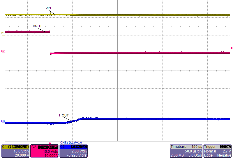
Transient: Output Short Circuit

4 Revision History
Changes from A Revision (August 2015) to B Revision
- Added section: Controlled Power Down using TPS25924xGo
Changes from * Revision (August 2015) to A Revision
- Changed from Product Preview to Production Data Go
5 Device Comparison Table
| PART NUMBER | UV | OV CLAMP | FAULT RESPONSE | STATUS |
|---|---|---|---|---|
| TPS259241 | 4.3 V | 15 V | Auto Retry | Active |
| TPS259240 | 4.3 V | 15 V | Latched | Active |
6 Pin Configuration and Functions

Pin Functions
| PIN | I/O | DESCRIPTION | |
|---|---|---|---|
| NAME | NO. | ||
| BFET | 9 | O | Connect this pin to the gate of a blocking NFET. See the Feature Description section. This pin can be left floating if it is not used |
| dV/dT | 1 | O | Tie a capacitor from this pin to GND to control the ramp rate of OUT at device turnon |
| EN/UVLO | 2 | I | This is a dual function control pin. When used as an ENABLE pin and pulled down, it shuts off the internal pass MOSFET and pulls BFET to GND. When pulled high, it enables the device and BFET. As an UVLO pin, it can be used to program different UVLO trip point via external resistor divider |
| GND | Thermal Pad | — | GND |
| ILIM | 10 | O | A resistor from this pin to GND sets the overload and short circuit limit |
| OUT | 6-8 | O | Output of the device |
| VIN | 3-5 | I | Input supply voltage |
7 Specifications
7.1 Absolute Maximum Ratings
over operating temperature range (unless otherwise noted) (1) (2)| MIN | MAX | UNIT | ||
|---|---|---|---|---|
| VIN | Supply voltage(1) | –0.3 | 20 | V |
| VIN (10-ms transient) | 22 | |||
| OUT | Output voltage | –0.3 | VIN + 0.3 | V |
| OUT (transient < 1 µs) | –1.2 | V | ||
| ILIM | Voltage | –0.3 | 7 | V |
| EN/UVLO | –0.3 | 7 | ||
| dV/dT | –0.3 | 7 | ||
| BFET | –0.3 | 30 | ||
| Tstg | Storage temperature | –65 | 150 | °C |
7.2 ESD Ratings
| VALUE | UNIT | |||
|---|---|---|---|---|
| V(ESD) | Electrostatic discharge | Human body model (HBM), per ANSI/ESDA/JEDEC JS-001(1) | ±2000 | V |
| Charged device model (CDM), per JEDEC specification JESD22-C101(2) | ±500 | |||
7.3 Recommended Operating Conditions
over operating free-air temperature range (unless otherwise noted)| MIN | TYP | MAX | UNIT | |||
|---|---|---|---|---|---|---|
| VIN | Input voltage | 4.5 | 12 | 13.8 | V | |
| BFET | 0 | VIN+6 | ||||
| dV/dT, EN/UVLO | 0 | 6 | ||||
| ILIM | 0 | 3 | ||||
| IOUT | Continuous output current | 0 | 5 | A | ||
| ILIM | Resistance | 10 | 100 | 162 | kΩ | |
| OUT | External capacitance | 0.1 | 1 | 1000 | µF | |
| dV/dT | 1 | 1000 | nF | |||
| TJ | Operating junction temperature | –40 | 25 | 125 | °C | |
| TA | Operating Ambient temperature | –40 | 25 | 85 | °C | |
7.4 Thermal Information
over operating free-air temperature range (unless otherwise noted)(1)| THERMAL METRIC | TPS25924x | UNIT | |
|---|---|---|---|
| DRC (VSON) | |||
| 10 PINS | |||
| RθJA | Junction-to-ambient thermal resistance | 45.9 | °C/W |
| RθJCtop | Junction-to-case (top) thermal resistance | 53 | °C/W |
| RθJB | Junction-to-board thermal resistance | 21.2 | °C/W |
| ψJT | Junction-to-top characterization parameter | 1.2 | °C/W |
| ψJB | Junction-to-board characterization parameter | 21.4 | °C/W |
| RθJCbot | Junction-to-case (bottom) thermal resistance | 5.9 | °C/W |
7.5 Electrical Characteristics
–40°C ≤ TJ ≤ +125°C, VIN = 12 V, VEN /UVLO = 2 V, RILIM = 100 kΩ, CdVdT = OPEN. All voltages referenced to GND (unless otherwise noted).| PARAMETER | TEST CONDITIONS | MIN | TYP | MAX | UNIT | |
|---|---|---|---|---|---|---|
| VIN (INPUT SUPPLY) | ||||||
| VUVR | UVLO threshold, rising | 4.15 | 4.3 | 4.45 | V | |
| VUVhyst | UVLO hysteresis(1) | 5% | ||||
| IQON | Supply current | Enabled: EN/UVLO = 2 V | 0.3 | 0.42 | 0.55 | mA |
| IQOFF | EN/UVLO = 0 V | 0.13 | 0.225 | mA | ||
| VOVC | Over-voltage clamp | VIN > 16.5 V, IOUT = 10 mA | 13.8 | 15 | 16.5 | V |
| EN/UVLO (ENABLE/UVLO INPUT) | ||||||
| VENR | EN threshold voltage, rising | 1.37 | 1.4 | 1.44 | V | |
| VENF | EN threshold voltage, falling | 1.32 | 1.35 | 1.39 | V | |
| IEN | EN Input leakage current | 0 V ≤ VEN ≤ 5 V | –100 | 0 | 100 | nA |
| dV/dT (OUTPUT RAMP CONTROL) | ||||||
| IdVdT | dV/dT charging current(1) | VdVdT = 0 V | 220 | nA | ||
| RdVdT_disch | dV/dT discharging resistance | EN/UVLO = 0 V, IdVdT = 10 mA sinking | 50 | 73 | 100 | Ω |
| VdVdTmax | dV/dT max capacitor voltage(1) | 5.5 | V | |||
| GAINdVdT | dV/dT to OUT gain(1) | ΔVdVdT | 4.85 | V/V | ||
| ILIM (CURRENT LIMIT PROGRAMMING) | ||||||
| IILIM | ILIM bias current(1) | 10 | µA | |||
| IOL | Overload current limit(2) | RILIM = 10 kΩ, VVIN-OUT = 1 V | 1.02 | A | ||
| RILIM = 45.3 kΩ, VVIN-OUT = 1 V | 1.79 | 2.10 | 2.42 | |||
| RILIM = 100 kΩ, VVIN-OUT = 1 V | 3.46 | 3.75 | 4.03 | |||
| RILIM = 150 kΩ, VVIN-OUT = 1 V | 4.5 | 5.1 | 5.7 | |||
| IOL-R-Short | RILIM = 0 Ω, shorted resistor current limit (single point failure test: UL60950)(1) | 0.84 | A | |||
| IOL-R-Open | RILIM = OPEN, open resistor current limit (single point failure test: UL60950)(1) | 0.73 | A | |||
| ISCL | Short-circuit current limit(2) | RILIM = 10 kΩ, VVIN-OUT = 12 V | 1 | A | ||
| RILIM = 45.3 kΩ, VVIN-OUT = 12 V | 1.66 | 1.98 | 2.37 | |||
| RILIM = 100 kΩ, VVIN-OUT = 12 V | 2.90 | 3.32 | 3.85 | |||
| RILIM = 150 kΩ, VVIN-OUT = 12 V | 3.7 | 4.5 | 5.5 | |||
| RATIOFASTRIP | Fast-trip comparator level w.r.t. overload current limit(1) | IFASTRIP : IOL | 160% | |||
| VOpenILIM | ILIM open resistor detect threshold(1) | VILIM rising, RILIM = OPEN | 3.1 | V | ||
| OUT (PASS FET OUTPUT) | ||||||
| RDS(on) | FET ON resistance | TJ = 25°C | 21 | 28 | 37 | mΩ |
| TJ = 125°C | 39 | 48 | ||||
| IOUT-OFF-LKG | OUT bias current in off state | VEN/UVLO = 0 V, VOUT = 0 V (sourcing) | –5 | 0 | 1.2 | µA |
| IOUT-OFF-SINK | VEN/UVLO = 0 V, VOUT = 300 mV (sinking) | 10 | 15 | 20 | ||
| BFET (BLOCKING FET GATE DRIVER) | ||||||
| IBFET | BFET charging current(1) | VBFET = VOUT | 2 | µA | ||
| VBFETmax | BFET clamp voltage(1) | VVIN + 6.4 | V | |||
| RBFETdisch | BFET discharging resistance to GND | VEN/UVLO = 0 V, IBFET = 100 mA | 15 | 26 | 36 | Ω |
| TSD (THERMAL SHUT DOWN) | ||||||
| TSHDN | TSD threshold, rising(1) | 150 | °C | |||
| TSHDNhyst | TSD hysteresis(1) | 10 | °C | |||
| Thermal fault: latched or auto-retry | TPS259240 | Latched | ||||
| TPS259241 | Auto-retry | |||||
7.6 Timing Requirements
| PARAMETER | TEST CONDITIONS | MIN | TYP | MAX | UNIT | |
|---|---|---|---|---|---|---|
| TON | Turnon delay(1) | EN/UVLO → H to IVIN = 100 mA, 1-A resistive load at OUT | 220 | µs | ||
| tOFFdly | Turnoff delay(1) | EN/UVLO↓ to BFET↓, CBFET = 0 | 0.4 | µs | ||
| dV/dT (OUTPUT RAMP CONTROL) | ||||||
| tdVdT | Output ramp time | EN/UVLO → H to OUT = 11.7 V, CdVdT = 0 | 0.7 | 1 | 1.3 | ms |
| EN/UVLO → H to OUT = 11.7 V, CdVdT = 1 nF(1) | 12 | |||||
| ILIM (CURRENT LIMIT PROGRAMMING) | ||||||
| tFastOffDly | Fast-Trip comparator delay(1) | IOUT > IFASTRIP to IOUT= 0 (Switch off) | 300 | ns | ||
| BFET (BLOCKING FET GATE DRIVER) | ||||||
| tBFET-ON | BFET Turnon duration(1) | EN/UVLO → H to VBFET = 12 V, CBFET = 1 nF | 4.2 | ms | ||
| EN/UVLO → H to VBFET = 12 V, CBFET = 10 nF | 42 | |||||
| tBFET-OFF | BFET Turnoff duration(1) | EN/UVLO → L to VBFET = 1 V, CBFET = 1 nF | 0.4 | µs | ||
| EN/UVLO → L to VBFET = 1 V, CBFET = 10 nF | 1.4 | |||||
| THERMAL SHUTDOWN (TSD) | ||||||
| tTSDdly | Retry delay after TSD recovery, TJ < [TSHDN - 10°C](1) | TPS259241 only | 100 | µs | ||
7.7 Typical Characteristics
TJ = 25°C, VVIN = 12 V, VEN/UVLO = 2 V, RILIM = 100 kΩ, CVIN = 0.1 µF, COUT = 1 µF, CdVdT = OPEN (unless stated otherwise)


| RILIM = 0 Ω | ||

| RILIM = 100 kΩ | ||

| RILIM = 150 kΩ | ||

| RILIM = 100 kΩ | ||


| CdVdT = 1nF, COUT = 10 µF, ROUT = 5.7Ω |

| EN ↓ | ||

| TPS259241 | ||

| ILOAD Stepped From 50% to 120%, back to 50% | ||

| RILIM = 150 kΩ | ||


| RILIM = OPEN | ||

| RILIM = 45.3 kΩ | ||

| RILIM = 150 kΩ | ||

| RILIM = 45.3 kΩ | ||


| CdVdT = OPEN, COUT = 4.7 µF |

| EN ↓ | ||

| VIN↓ | ||

| TPS259241 | ||

| RILIM = 150 kΩ | ||

