-
TPS31xx Ultralow Supply-Current Voltage Monitor With Optional Watchdog
- 1 Features
- 2 Applications
- 3 Description
- 4 Revision History
- 5 Available Options
- 6 Pin Configuration and Functions
- 7 Specifications
- 8 Detailed Description
- 9 Application and Implementation
- 10Power Supply Recommendations
- 11Layout
- 12Device and Documentation Support
- 13Mechanical, Packaging, and Orderable Information
- IMPORTANT NOTICE
Package Options
Refer to the PDF data sheet for device specific package drawings
Mechanical Data (Package|Pins)
- DBV|6
Thermal pad, mechanical data (Package|Pins)
Orderable Information
TPS31xx Ultralow Supply-Current Voltage Monitor With Optional Watchdog
1 Features
-
Precision Supply Voltage Supervision Range:
0.9 V, 1.2 V, 1.5 V, 1.6 V, 2 V, and 3.3 V - High Trip-Point Accuracy: 0.75%
- Supply Current of 1.2 μA (Typical)
- RESET Defined With Input Voltages as Low as 0.4 V
- Power-On Reset Generator With a Delay Time of 130 ms
- Push/Pull or Open-Drain RESET Outputs
- Package Temperature Range: –40°C to 125°C
2 Applications
- Applications Using Low-Power DSPs, Microcontrollers, or Microprocessors
- Portable and Battery-Powered Equipment
- Intelligent Instruments
- Wireless Communication Systems
- Industrial Equipment
- Notebook and Desktop Computers
3 Description
The TPS310x and TPS311x families of supervisory circuits provide circuit initialization and timing supervision, primarily for DSP and processor-based systems.
During power-on, RESET is asserted low when the supply voltage (VDD) becomes higher than 0.4 V. Thereafter, the supervisory circuit monitors VDD and keeps the RESET output low as long as VDD remains below the threshold voltage (VIT–). To ensure proper system reset, after VDD surpasses the threshold voltage, an internal timer delays the transition of the RESET signal from low to high for the specified time. When VDD drops below VIT–, the output transitions low again.
All the devices of this family have a fixed-sense threshold voltage (VIT–) set by an internal voltage divider.
The TPS3103 and TPS3106 devices have an active-low, open-drain RESET output and either an integrated power-fail input (PFI) or SENSE input with corresponding outputs for monitoring other voltages. The TPS3110 has an active-low push/pull RESET and a watchdog timer to monitor the operation of microprocessors. All three devices have a manual reset pin that can be used to force the outputs low regardless of the sensed voltages.
The product spectrum is designed for supply voltages of 0.9 V up to 3.6 V. The circuits are available in 6-pin SOT-23 packages. The TPS31xx family is characterized for operation over a temperature range of –40°C to 125°C.
Device Information(1)
| PART NUMBER | PACKAGE | BODY SIZE (NOM) |
|---|---|---|
| TPS3103xxx | SOT-23 (6) | 2.90 mm × 1.60 mm |
| TPS3106xxx | ||
| TPS3110xxx |
- For all available packages, see the orderable addendum at the end of the data sheet.
4 Revision History
Changes from F Revision (November 2015) to G Revision
- Changed Package Temperature Range Features bullet to extend to 125°C Go
- Changed supply voltage and temperature range in last paragraph of Description section Go
- Changed maximum specifications in Supply voltage, All other pins, and Operating temperature parameters in Absolute Maximum Ratings tableGo
- Changed maximum specifications in VDD, PFI, and TJ parameters of Recommended Operating Conditions tableGo
- Added TA = –40°C to 125°C rows to VIT– parameter of Electrical Characteristics tableGo
- Added second row to VIT–(S) parameter of Electrical Characteristics tableGo
- Changed IDD parameter of Electrical Characteristics tableGo
- Changed Typical Characteristics curves TPS3110E09 Supply Current vs Supply Voltage, TPS3110E09 Low-Level Output Voltage vs Low-Level Output Current, TPS3110E09 Low-Level Output Voltage vs Low-Level Output Current, TPS3110E09 High-Level Output Voltage vs High-Level Output Current, and TPS3110K33 High-Level Output Voltage vs High-Level Output Current Go
- Changed Normalized Threshold Voltage vs Free-Air Temperature curveGo
- Changed supply voltage range in first sentence of Overview section Go
- Changed supply voltage range in description of Application Information section Go
- Changed Normalized Threshold Voltage vs Free-Air Temperature figureGo
- Changed supply voltage range in first sentence of Power Supply Recommendations sectionGo
Changes from E Revision (September 2007) to F Revision
- Added ESD Ratings table, Feature Description section, Device Functional Modes, Application and Implementation section, Power Supply Recommendations section, Layout section, Device and Documentation Support section, and Mechanical, Packaging, and Orderable Information section Go
- Changed title of document Go
- Deleted Features bullet for SOT23-6 package Go
- Changed front-page figureGo
- Changed second paragraph of Description section Go
- Changed fourth paragraph of Description sectionGo
- Changed Pin Configuration and Functions section; updated table format Go
- Changed "free-air temperature" to "junction temperature" in Absolute Maximum Ratings condition statementGo
- Deleted clamp current from Absolute Maximum Ratings table; changed to currentGo
- Deleted soldering temperature specification from Absolute Maximum Ratings tableGo
- Changed "free-air temperature" to "junction temperature" in Recommended Operating Conditions condition statement Go
- Added Thermal Information table; deleted Dissipation Ratings tableGo
- Changed "free-air temperature" to "junction temperature" in Electrical Characteristics condition statement Go
- Changed Switching Characteristics tableGo
- Changed Figure 1 title and timing drawing Go
- Changed Figure 2 titleGo
- Changed Figure 3Go
- Changed Figure 4Go
5 Available Options
| DEVICE | RESET OUTPUT | RSTSENSE, RSTVDD OUTPUT | SENSE INPUT | WDI INPUT | PFO OUTPUT |
|---|---|---|---|---|---|
| TPS3103 | Open-drain | Open-drain | |||
| TPS3106 | Open-drain | ✓ | |||
| TPS3110 | Push-pull | ✓ | ✓ |
6 Pin Configuration and Functions


Pin Functions
7 Specifications
7.1 Absolute Maximum Ratings
over operating junction temperature range (unless otherwise noted)(1)| MIN | MAX | UNIT | ||
|---|---|---|---|---|
| Supply voltage(2) | VDD | –0.3 | 4 | V |
| MR Pin, RESET (push-pull) | VMR, VRESET (push-pull) | –0.3 | VDD + 0.3 | V |
| All other pins(2) | –0.3 | 4 | V | |
| Maximum low output current | IOL | –5 | 5 | mA |
| Maximum high output current | IOH | –5 | 5 | mA |
| Input current | IIK (VSENSE < 0 V or VSENSE > VDD) | –10 | 10 | mA |
| Output current | IOK (VO < 0 V or VO > VDD)(3) | –10 | 10 | mA |
| Continuous total power dissipation | See Thermal Information | |||
| Temperature | Operating, TJ | –40 | 125 | °C |
| Storage, Tstg | –65 | 150 | °C | |
7.2 ESD Ratings
| VALUE | UNIT | |||
|---|---|---|---|---|
| V(ESD) | Electrostatic discharge | Human body model (HBM), per ANSI/ESDA/JEDEC JS-001, all pins(1) | ±2000 | V |
| Charged device model (CDM), per JEDEC specification JESD22-C101, all pins(2) | ±500 | |||
7.3 Recommended Operating Conditions
over operating junction temperature range, unless otherwise noted.| MIN | NOM | MAX | UNIT | ||
|---|---|---|---|---|---|
| VDD(1) | Supply voltage | 0.9 | 3.6 | V | |
| VSENSE | SENSE voltage | 0 | VDD | V | |
| WDI | High-level input voltage VIH at MR | 0.7 × VDD | V | ||
| WDI | Low-level input voltage VIL at MR | 0.3 × VDD | V | ||
| WDI | Input transition rise and fall rate at Δt/ΔV at MR | 100 | ns/V | ||
| MR | MR voltage | 0 | VDD | V | |
| PFI | PFI voltage | 0 | 3.6 | V | |
| TJ | Operating temperature | –40 | 125 | °C | |
7.4 Thermal Information
| THERMAL METRIC(1) | TPS31xx | UNIT | |
|---|---|---|---|
| DBV (SOT-23) | |||
| 6 PINS | |||
| RθJA | Junction-to-ambient thermal resistance | 183.2 | °C/W |
| RθJC(top) | Junction-to-case (top) thermal resistance | 123.3 | °C/W |
| RθJB | Junction-to-board thermal resistance | 29.4 | °C/W |
| ψJT | Junction-to-top characterization parameter | 20.5 | °C/W |
| ψJB | Junction-to-board characterization parameter | 29 | °C/W |
7.5 Electrical Characteristics
over operating junction temperature range (unless otherwise noted).| PARAMETER | TEST CONDITIONS | MIN | TYP | MAX | UNIT | ||
|---|---|---|---|---|---|---|---|
| VOH | High-level output voltage | VDD = 3.3 V, IOH = –3 mA | 0.8 × VDD | V | |||
| VDD = 1.8 V, IOH = –2 mA | |||||||
| VDD = 1.5 V, IOH = –1 mA | |||||||
| VDD = 0.9 V, IOH = –0.4 mA | |||||||
| VDD = 0.5 V, IOH = –5 μA | 0.7 × VDD | ||||||
| VOL | Low-level output voltage | VDD = 3.3 V, IOL = 3 mA | 0.3 | V | |||
| VDD = 1.5 V, IOL = 2 mA | |||||||
| VDD = 1.2 V, IOL = 1 mA | |||||||
| VDD = 0.9 V, IOL = 500 μA | |||||||
| VOL | Low-level output voltage | RESET only | VDD = 0.4 V, IOL = 5 μA | 0.1 | V | ||
| VIT– | Negative-going input threshold voltage(1) | TPS31xxE09 | TA = 25°C | 0.854 | 0.86 | 0.866 | V |
| TPS31xxE12 | 1.133 | 1.142 | 1.151 | ||||
| TPS31xxE15 | 1.423 | 1.434 | 1.445 | ||||
| TPS31xxE16 | 1.512 | 1.523 | 1.534 | ||||
| TPS31xxH20 | 1.829 | 1.843 | 1.857 | ||||
| TPS31xxK33 | 2.919 | 2.941 | 2.963 | ||||
| TPS31xxE09 | TA = –40°C to 125°C | 0.817 | 0.903 | ||||
| TPS31xxE12 | 1.084 | 1.199 | |||||
| TPS31xxE15 | 1.362 | 1.505 | |||||
| TPS31xxK33 | 2.823 | 3.058 | |||||
| VIT–(S) | Negative-going input threshold voltage(1) | SENSE, PFI | VDD ≥ 0.8 V, TA = 25°C | 0.542 | 0.551 | 0.559 | V |
| VDD ≥ 0.8 V, TA = –40°C to 125°C | 0.5 | 0.58 | |||||
| VHYS | Hysteresis at VDD input | 0.8 V ≤ VIT– < 1.5 V | 20 | mV | |||
| 1.6 V ≤ VIT– < 2.4 V | 30 | ||||||
| 2.5 V ≤ VIT– < 3.3 V | 50 | ||||||
| T(K) | Temperature coefficient of VIT−, PFI, SENSE | TA = –40°C to 85°C | –0.012 | –0.019 | %/K | ||
| VHYS(S) | Hysteresis at SENSE, PFI input | VDD ≥ 0.8 V | 15 | mV | |||
| IIH | High-level input current | MR | MR = VDD, VDD = 3.3 V | –25 | 25 | nA | |
| SENSE, PFI, WDI | SENSE, PFI, WDI = VDD, VDD = 3.3 V |
–25 | 25 | ||||
| IIL | Low-level input current | MR | MR = 0 V, VDD = 3.3 V | –47 | –33 | –25 | μA |
| SENSE, PFI, WDI | SENSE, PFI, WDI = 0 V, VDD = 3.3 V |
–25 | 25 | nA | |||
| IOH | High-level output current at RESET(2) | Open-drain | VDD = VIT– + 0.2 V, VOH = 3.3 V | 200 | nA | ||
| IDD | Supply current | TA = –40°C to 85°C, VDD > VIT– (average current), VDD < 1.8 V | 1.2 | 3 | μA | ||
| TA = –40°C to 125°C, VDD > VIT– (average current), VDD < 1.8 V | 3 | ||||||
| TA = –40°C to 85°C, VDD > VIT– (average current), VDD > 1.8 V | 2 | 4.5 | |||||
| TA = –40°C to 125°C, VDD > VIT– (average current), VDD > 1.8 V | 5.5 | ||||||
| TA = –40°C to 85°C, VDD < VIT–, VDD < 1.8 V | 22 | ||||||
| TA = –40°C to 125°C, VDD < VIT–, VDD < 1.8 V | 27 | ||||||
| TA = –40°C to 85°C, VDD < VIT–, VDD > 1.8 V | 27 | ||||||
| TA = –40°C to 125°C, VDD < VIT–, VDD > 1.8 V | 32 | ||||||
| Internal pullup resistor at MR | 70 | 100 | 130 | kΩ | |||
| CIN | Input capacitance at MR, SENSE, PFI, WDI | VIN = 0 V to VDD | 1 | pF | |||
7.6 Timing Requirements
At RL = 1 MΩ, CL = 50 pF, and TA = –40°C to 85°C, unless otherwise noted.| MIN | TYP | MAX | UNIT | ||||
|---|---|---|---|---|---|---|---|
| tT(OUT) | Time-out period | at WDI | VDD ≥ 0.85 V | 0.55 | 1.1 | 1.65 | s |
| tW | Pulse duration | at VDD | VIH = 1.1 × VIT–, VIL = 0.9 × VIT–, VIT– = 0.86 V | 20 | μs | ||
| at MR | VDD ≥ VIT– + 0.2 V, VIL = 0.3 × VDD, VIH = 0.7 × VDD | 0.1 | |||||
| at SENSE | VDD ≥ VIT–, VIH = 1.1 × VIT − (S), VIL = 0.9 × VIT − (S) | 20 | |||||
| at PFI | VDD ≥ 0.85 V, VIH = 1.1 × VIT − (S),VIL = 0.9 × VIT − (S) | 20 | |||||
| at WDI | VDD ≥ VIT–, VIL = 0.3 × VDD, VIH = 0.7 × VDD | 0.3 | |||||
7.7 Switching Characteristics
At RL = 1 MΩ, CL = 50 pF, and TA = –40°C to 85°C, unless otherwise noted.| PARAMETER | TEST CONDITIONS | MIN | TYP | MAX | UNIT | ||
|---|---|---|---|---|---|---|---|
| tD | Delay time | VDD ≥ 1.1 × VIT–, MR = 0.7 × VDD. See Timing Requirements. |
65 | 130 | 195 | ms | |
| tPHL(VDD) | Propagation delay time, high-to-low level output |
VDD to RESET or RSTVDD delay | VIH = 1.1 × VIT–, VIL = 0.9 × VIT– | 40 | μs | ||
| tPHL(SENSE) | Propagation delay time, high-to-low level output |
SENSE to RESET or RSTSENSE delay | VDD ≥ 0.8 V, VIH = 1.1 × VIT–, VIL = 0.9 × VIT– | 40 | μs | ||
| tPHL(PFO) | Propagation delay time, high-to-low level output |
PFI to PFO delay | VDD ≥ 0.8 V, VIH = 1.1 × VIT–, VIL = 0.9 × VIT– | 40 | μs | ||
| tPLH(PFO) | Propagation delay time, low-to-high level output |
PFI to PFO delay | VDD ≥ 0.8 V, VIH = 1.1 × VIT–, VIL = 0.9 × VIT– | 300 | μs | ||
| tPHL(MR) | Propagation delay time, high-to-low level output |
MR to RESET. RSTVDD, RSTSENSE delay | VDD ≥ 1.1 × VIT–, VIL = 0.3 × VDD, VIH = 0.7 × VDD | 1 | 5 | μs | |
7.8 Typical Characteristics
 Figure 5. TPS3110E09 Supply Current vs Supply Voltage

| VDD = 3.3 V, SENSE = GND, MR = GND, WDI: GND |
Low-Level Output Current

| VDD = 3.3 V, SENSE = VDD, MR = VDD, WDI: triggered |
High-Level Output Current

| VDD = 0.9 V, SENSE = GND, MR = GND, WDI: GND |
Low-Level Output Current

| VDD = 0.9 V, SENSE = VDD, MR = VDD, WDI: triggered |
High-Level Output Current

Threshold Overdrive Voltage
8 Detailed Description
8.1 Overview
The TPS310x and TPS311x families of supervisory circuits operate from supply voltages from 0.9 V to 3.6 V and provide circuit initialization and timing supervision for DSP- and processor-based systems. During power-on, RESET is asserted when the supply voltage (VDD) exceeds 0.4 V. The devices monitor VDD and keep the RESET output low as long as VDD remains below the threshold voltage (VIT–). To ensure proper system reset, after VDD surpasses the threshold voltage plus the hysteresis (VIT– + VHYS) an internal timer delays the transition of the RESET signal from low to high for the specified time. The delay time starts after VDD has risen above (VIT– + VHYS). When VDD drops below VIT–, the output becomes active again.
All the devices of this family have a fixed-VDD threshold voltage (VIT–) set by an internal voltage divider. The TPS3103 and TPS3106 devices both have an active-low, open-drain RESET output. The TPS3103 device has an integrated power-fail input (PFI) and corresponding power-fail output (PFO) that can be used for low-battery detection or for monitoring a power supply other than the input supply. The TPS3106 device has a SENSE input with a corresponding output (RSTSENSE) for monitoring voltages other than the input supply. The TPS3110 device has an active-low push/pull RESET and a watchdog timer that is used for monitoring the operation of microprocessors. All three devices have manual reset pin (MR) that can be used to force the outputs low regardless of the sensed voltages.
8.2 Functional Block Diagrams
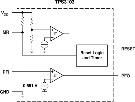 Figure 12. TPS3103 Functional Block Diagram
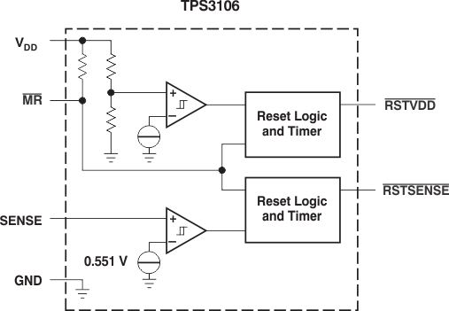 Figure 13. TPS3106 Functional Block Diagram
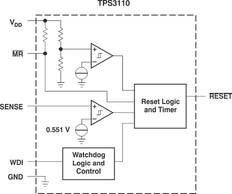 Figure 14. TPS3110 Functional Block Diagram
8.3 Feature Description
8.3.1 Watchdog
The TPS3110 device integrates a watchdog timer that must be periodically triggered by a positive or negative transition of WDI. When the supervising system fails to retrigger the watchdog circuit within the time-out interval, RESET becomes active for the time period (tD). This event also reinitializes the watchdog timer.
8.3.2 Manual Reset (MR)
Many μC-based products require manual-reset capability, allowing an operator or logic circuitry to initiate a reset. Logic low at MR asserts reset. Reset remains asserted while MR is low and for a time period (tD) after MR returns high. The input has an internal 100-kΩ pullup resistor, so it can be left open if it is unused.
Connect a normally open momentary switch from MR to GND to create a manual reset function. External debounce is not required. If MR is driven from long cables or if the device is used in noisy environments, connecting a 0.1-μF capacitor from MR to GND provides additional noise immunity.
If there is a possibility of transient or DC conditions causing MR to rise above VDD, a diode should be used to limit MR to a diode drop above VDD.
8.3.3 PFI, PFO
The TPS3103 has an integrated power-fail (PFI) comparator with a separate open-drain (PFO) output. The PFI and PFO can be used for low-battery detection, power-fail warning, or for monitoring a power supply other than the main supply, and has no effect on RESET.
An additional comparator is provided to monitor voltages other than the nominal supply voltage. The power-fail input (PFI) will be compared with an internal voltage reference of 0.551 V. If the input voltage falls below the power-fail threshold (VIT – (S)), the power-fail output (PFO) goes low. If it goes above 0.551 V plus approximately 15-mV hysteresis, the output returns to high. By connecting two external resistors, it is possible to supervise any voltage above 0.551 V. The sum of both resistors should be approximately 1 MΩ, to minimize power consumption and to assure that the current into the PFI pin can be neglected, compared with the current through the resistor network. The tolerance of the external resistors should be not more than 1% to ensure minimal variation of sensed voltage. If the power-fail comparator is unused, connect PFI to GND and leave PFO unconnected. For proper operation of the PFI-comparator, the supply voltage (VDD) must be higher than 0.8 V.
8.3.4 SENSE
The voltage at the SENSE input is compared with a reference voltage of 0.551 V. If the voltage at SENSE falls below the sense-threshold (VIT − (S)), reset is asserted. On the TPS3106 device, a dedicated RSTSENSE output is available. On the TPS3110 device, the logic signal from SENSE is OR-wired with the logic signal from VDD or MR. An internal timer delays the return of the output to the inactive state, once the voltage at SENSE goes above 0.551 V plus about 15 mV of hysteresis. For proper operation of the SENSE-comparator, the supply voltage must be higher than 0.8 V.
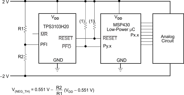
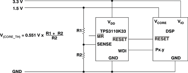 Figure 16. TPS3110 in a DSP-System Monitoring Both Supply Voltages
8.4 Device Functional Modes
Table 1. TPS3103 Function Table
| MR | V(PFI) > 0.551 V | VDD > VIT– | RESET | PFO |
|---|---|---|---|---|
| L | 0 | X(1) | L | L |
| L | 1 | X | L | H |
| H | 0 | 0 | L | L |
| H | 0 | 1 | H | L |
| H | 1 | 0 | L | H |
| H | 1 | 1 | H | H |
Table 2. TPS3106 Function Table
| MR | V(SENSE) > 0.551 V | VDD > VIT– | RSTVDD | RSTSENSE |
|---|---|---|---|---|
| L | X(1) | X | L | L |
| H | 0 | 0 | L | L |
| H | 0 | 1 | H | L |
| H | 1 | 0 | L | H |
| H | 1 | 1 | H | H |


