-
TPS386596 Quad Reset Supervisor With Manual Reset Input
- 1 Features
- 2 Applications
- 3 Description
- 4 Revision History
- 5 Pin Configuration and Functions
- 6 Specifications
- 7 Parameter Measurement Information
- 8 Detailed Description
- 9 Application and Implementation
- 10Power Supply Recommendations
- 11Layout
- 12Device and Documentation Support
- 13Mechanical, Packaging, and Orderable Information
- IMPORTANT NOTICE
Package Options
Mechanical Data (Package|Pins)
- DGK|8
Thermal pad, mechanical data (Package|Pins)
Orderable Information
TPS386596 Quad Reset Supervisor With Manual Reset Input
1 Features
- Four Channel Voltage Detector
- Threshold Accuracy: 0.25% (typ)
- Fixed 50-ms RESET Delay Time
- Active-Low Manual Reset Input
- Very Low Quiescent Current: 7 µA (Typical)
- SVS-1: Fixed Threshold for Monitoring 3.3 V
- SVS-2/3/4: Adjustable Threshold Down to 0.4 V
- Open-Drain RESET Output
- Space-Saving, 8-pin MSOP Package
2 Applications
- Notebook/Desktop Computers
- Industrial Equipment
- Telecom, Networking Infrastructure
- Server, Storage Equipment
- DSP and Microcontroller Applications
- FPGA/ASIC Applications
3 Description
The TPS386596 device monitors four power rails and asserts the RESET signal when any of the SENSE inputs drop below the respective thresholds. SVS-1 can be used to monitor a 3.3-V nominal power supply with no external components required. SVS-2, SVS-3, and SVS-4 are adjustable using external resistors and can be used to monitor any power-supply voltage higher than 0.4 V. All SENSE inputs have a threshold accuracy of 0.25% (typical). The TPS386596L33 also has an active-low manual reset (MR) that can assert the RESET signal as desired by the application. The open-drain, active-low RESET output deasserts after a fixed 50-ms delay.
The TPS386596 has a low quiescent current of 7 µA (typical) and is available in a space-saving, 8-pin MSOP package.
Device Information(1)
| PART NUMBER | PACKAGE | BODY SIZE (NOM) |
|---|---|---|
| TPS386596 | VSSOP (8) | 5.00 mm × 3.00 mm |
- For all available packages, see the orderable addendum at the end of the data sheet.
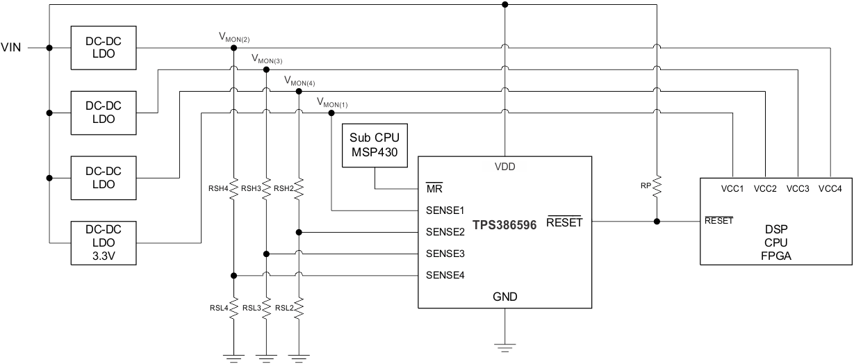
TPS386596 Typical Application Circuit
4 Revision History
Changes from * Revision (July 2010) to A Revision
- Changed references to TPS386596L33 to TPS386596 throughout documentGo
- Changed Pin Configuration and Functions section; updated table format and pin drawing Go
- Changed "free-air temperature" to "junction temperature" in Absolute Maximum Ratings condition statementGo
- Changed Absolute Maximum Ratings table; moved ESD ratings to separate table Go
- Added ESD Ratings table, Feature Description section, Device Functional Modes, Application and Implementation section, Power Supply Recommendations section, Layout section, Device and Documentation Support section, and Mechanical, Packaging, and Orderable Information section Go
- Changed Thermal Information table; updated thermal resistance valuesGo
- Changed Electrical Characteristics table; moved timing and switching parameters (tW, tD) to separate tablesGo
- Changed input voltage range notation from VVCC to VDDthroughout Electrical Characteristics tableGo
- Changed supply current notation from IVCC to IDD in Electrical Characteristics tableGo
- Changed VCC notation in Functional Block Diagram to VDDGo
- Deleted Immunity to SENSE Pin Voltage Transients section; rewrote content and added to Voltage Monitoring section Go
- Changed Sense Inputs section title to Undervoltage DetectionGo
- Changed title and graphic for Figure 14Go
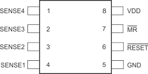
5 Pin Configuration and Functions
Pin Functions
| PIN | I/O | DESCRIPTION | ||
|---|---|---|---|---|
| NAME | NO. | |||
| GND | 5 | — | Ground | |
| MR | 7 | I | Manual reset input with internal 100-kΩ pullup to VDD and 50-ns deglitch. Logic low level of this pin asserts RESET. | |
| RESET | 6 | O | RESET is an open-drain output pin. When RESET is asserted, this pin remains in a low-impedance state. When RESET is deasserted, this pin goes to a high-impedance state after 50 ms. A pullup resistor to VDD or another voltage source is required. | |
| SENSE1 | 4 | I | Monitor voltage input for Supply 1 | When the voltage at this terminal drops the threshold voltage (VIT1= 2.9 V), RESET is asserted. |
| SENSE2 | 3 | I | Monitor voltage input for Supply 2 | When the voltage at this terminal drops the threshold voltage (VIT2= 0.4 V), RESET is asserted. |
| SENSE3 | 2 | I | Monitor voltage input for Supply 3 | When the voltage at this terminal drops the threshold voltage (VIT3= 0.4 V), RESET is asserted. |
| SENSE4 | 1 | I | Monitor voltage input for Supply 4 | When the voltage at this terminal drops the threshold voltage (VIT4= 0.4 V), RESET is asserted. |
| VDD | 8 | I | Supply voltage. Connecting a 0.1-µF ceramic capacitor close to this pin is recommended. | |
6 Specifications
6.1 Absolute Maximum Ratings
over operating junction temperature range (unless otherwise noted).(1)(2)| MIN | MAX | UNIT | ||
|---|---|---|---|---|
| Voltage | Input, VDD | –0.3 | 7 | V |
| VMR, VSENSE1, VSENSE2, VSENSE3, VSENSE4, VRESET | –0.3 | 7 | V | |
| Current | RESET pin | 5 | mA | |
| Power dissipation | Continuous total | See Thermal Information | ||
| Temperature | Operating virtual junction, TJ | –40 | 150 | °C |
| Operating ambient, TA | –40 | 125 | ||
| Storage, Tstg | –65 | 150 | ||
6.2 ESD Ratings
| VALUE | UNIT | |||
|---|---|---|---|---|
| V(ESD) | Electrostatic discharge | Human body model (HBM), per ANSI/ESDA/JEDEC JS-001(1) | ±2000 | V |
| Charged-device model (CDM), per JEDEC specification JESD22-C101(2) | ±500 | |||
6.3 Recommended Operating Conditions
Over operating junction temperature range (unless otherwise noted).| MIN | NOM | MAX | UNIT | ||
|---|---|---|---|---|---|
| VDD | 1.8 | 6.5 | V | ||
| VSENSE(1) | 0 | VDD | V | ||
| VMR | 0 | VDD | V | ||
| VRESET | 0 | 6.5 | V | ||
| RPULL-UP | 6.5 | 100 | 10,000 | kΩ | |
| TJ | –40 | 25 | 125 | °C | |
6.4 Thermal Information
| THERMAL METRIC(1) | TPS386596 | UNIT | |
|---|---|---|---|
| DGK (VSSOP) | |||
| 8 PINS | |||
| RθJA | Junction-to-ambient thermal resistance | 174 | °C/W |
| RθJC(top) | Junction-to-case (top) thermal resistance | 45.5 | °C/W |
| RθJB | Junction-to-board thermal resistance | 94 | °C/W |
| ψJT | Junction-to-top characterization parameter | 1.9 | °C/W |
| ψJB | Junction-to-board characterization parameter | 92.7 | °C/W |
| RθJC(bot) | Junction-to-case (bottom) thermal resistance | N/A | °C/W |
6.5 Electrical Characteristics
Over the operating temperature range of TJ = –40°C to 125°C. 1.8 V < VDD < 6.5 V, RRESET = 100 kΩ to VDD, CRESET = 50 pF to GND, unless otherwise noted. Typical values are at TJ = 25°C.| PARAMETER | TEST CONDITIONS | MIN | TYP | MAX | UNIT | |
|---|---|---|---|---|---|---|
| VDD | Input supply | 1.8 | 6.5 | V | ||
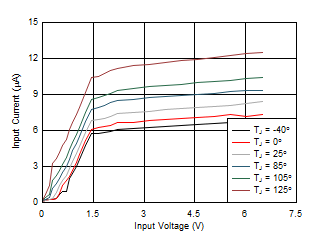
| IDD | Supply current (current into VDD pin) | VCC = 3.3 V, RESET not asserted | 7 | 19 | µA | |
| VCC = 6.5 V, RESET not asserted | 7.5 | 22 | µA | |||
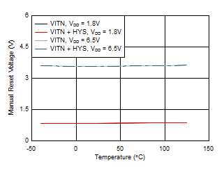
| Power-on reset voltage(1)(2) | VOL(max) = 0.2 V, IRESET = 15 µA | 0.9 | V | |||
| VITn | Negative-going input threshold accuracy | SENSE1 | 2.87 | 2.90 | 2.93 | V |
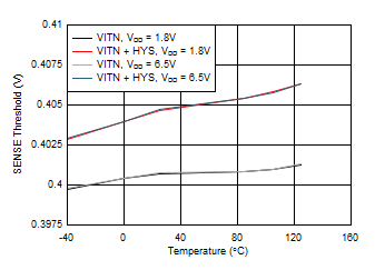
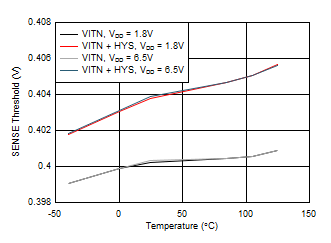
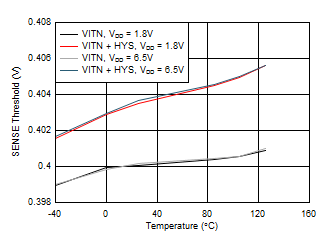
| SENSE2, SENSE3, SENSE4 | 396 | 400 | 404 | mV | ||
| VHYS | Hysteresis (positive-going) on VITn | SENSE1 | 25 | 72 | mV | |
| SENSE2, SENSE3, SENSE4 | 3.5 | 10 | mV | |||
| ISENSE1 | Input current at SENSE1 | VSENSE1 = 3.3 V | 2.2 | 2.75 | 3.3 | µA |
| ISENSEn | Input current at SENSEn pin, n = 2, 3, 4 |
VSENSEn = 0.42 V | –25 | 25 | nA | |
| td | RESETdelay time | 30 | 50 | 70 | ms | |
| VIL | MR logic low input | 0 | 0.3VDD | V | ||
| VIH | MR logic high input | 0.7VDD | V | |||
| RMR_Pullup | Internal pullup resistor on MR pin to VDD | 100 | kΩ | |||
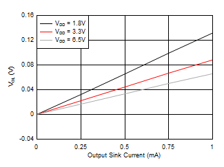
| VOL | Low-level RESET output voltage | IOL = 1 mA | 0.4 | V | ||
| SENSEn = 0 V, 1.3 V < VDD < 1.8 V, IOL = 0.4 mA(1) |
0.3 | |||||
| ILKG | RESET leakage current | VRESET = 6.5 V, RESET not asserted | –300 | 300 | nA | |
| CIN | Input pin capacitance | 5 | pF | |||
6.6 Timing Requirements
Over the operating temperature range of TJ = –40°C to 125°C. 1.8 V < VDD < 6.5 V, RRESET = 100 kΩ to VDD, CRESET = 50 pF to GND, unless otherwise noted. Typical values are at TJ = 25°C.| MIN | NOM | MAX | UNIT | |||
|---|---|---|---|---|---|---|
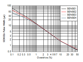
| tW | Input pulse width to SENSEn and MR pins | SENSEm: 1.05 VIT ≥ 0.95 VIT | 4 | μs | ||
| MR: 0.7 VDD ≥ 0.3 VDD | 50 | ns | ||||
6.7 Switching Characteristics
Over the operating temperature range of TJ = –40°C to 125°C. 1.8 V < VDD < 6.5 V, RRESET = 100 kΩ to VDD, CRESET = 50 pF to GND, unless otherwise noted. Typical values are at TJ = 25°C.| MIN | TYP | MAX | UNIT | |||
|---|---|---|---|---|---|---|
| tD | RESET delay time | 30 | 50 | 70 | ms | |
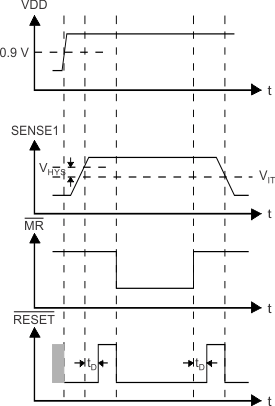 Figure 1. Timing Diagram
6.8 Typical Characteristics
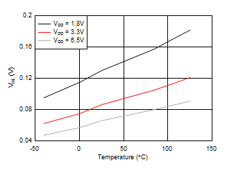
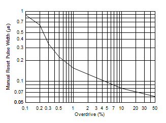
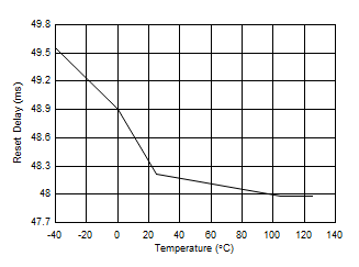
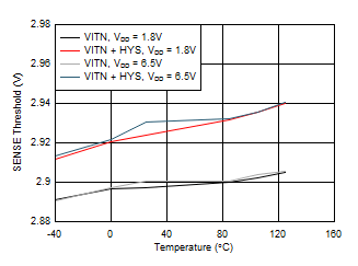
At TA = 25°C, and VDD = 3.3 V, unless otherwise noted.