SLVSCT3 March 2015 TPS51275B-1
PRODUCTION DATA.
- 1 Features
- 2 Applications
- 3 Description
- 4 Typical Application Diagram
- 5 Revision History
- 6 Pin Configuration and Functions
- 7 Specifications
-
8 Detailed Description
- 8.1 Overview
- 8.2 Functional Block Diagram
- 8.3
Feature Description
- 8.3.1 PWM Operations
- 8.3.2 Adaptive On-Time and PWM Frequency Control
- 8.3.3 Light-Load Condition in Out-of-Audio Operation
- 8.3.4 Enable and Power Good
- 8.3.5 Soft-Start and Discharge
- 8.3.6 VREG5 and VREG3 Linear Regulators
- 8.3.7 VCLK for Charge Pump
- 8.3.8 Overcurrent Protection
- 8.3.9 Output Overvoltage and Undervoltage Protection
- 8.3.10 Undervoltage Lockout Protection
- 8.3.11 Over-Temperature Protection (OTP)
- 8.4 Device Functional Modes
- 9 Application and Implementation
- 10Power Supply Recommendations
- 11Layout
- 12Device and Documentation Support
- 13Mechanical, Packaging, and Orderable Information
Package Options
Mechanical Data (Package|Pins)
- RUK|20
Thermal pad, mechanical data (Package|Pins)
- RUK|20
Orderable Information
1 Features
- Input Voltage Range: 5 V to 24 V
- Output Voltages: 5 V and 3.3 V (Adjustable Range ±10%)
- Built-in, 100-mA, 5-V, and 3.3-V LDOs
- Clock Output for Charge-Pump
- ±1% Reference Accuracy
- Adaptive On-Time D-CAP™ Mode Control Architecture with 300-kHz and 355-kHz Frequency Setting
- Out-of-Audio™ (OOA) Light-Load Operation
- Internal 3.2-ms Voltage Servo Soft-Start
- Low-Side RDS(on) Current Sensing Scheme
- Built-In Output Discharge Function
- Separate Enable Input for Switchers
- Dedicated OC Setting Terminals
- Power Good Indicator
- OVP, UVP, and OCP Protection
- Non-Latch UVLO and OTP Protection
- 20-Pin, 3-mm × 3-mm, WQFN (RUK) Package
2 Applications
- Notebook Computers
- Tablet Computers
- Desktop Computers
3 Description
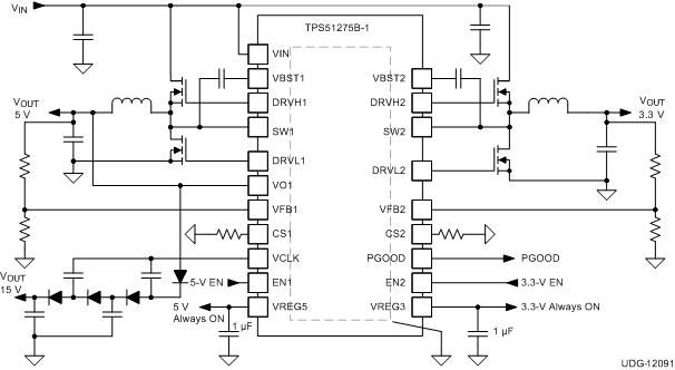
The TPS51275B-1 device is a cost-effective, dual-synchronous buck controller targeted for notebook system-power supply solutions. The device has 5-V and 3.3-V low-dropout regulators (LDOs) and requires few external components. The 260-kHz VCLK output can be used to drive an external charge pump, generating gate drive voltage for the load switches without reducing the main converter efficiency. The TPS51275B-1 device supports high efficiency, fast transient response and provides a combined power-good signal. Adaptive on-time, D-CAP control provides convenient and efficient operation. The device operates with a supply input voltage ranging from 5 to 24 V and supports output voltages of 5 V and 3.3 V. The TPS51275B-1 device is available in a 20-pin, 3-mm × 3-mm, WQFN package and is specified from –40°C to 85°C.
Device Information(1)
| PART NUMBER | SKIP MODE | ALWAYS ON-LDO |
|---|---|---|
| TPS51275B-1 | OOA | VREG3 and VREG5 |
- For all available packages, see the orderable addendum at the end of the datasheet.
4 Typical Application Diagram
