SLVSBB7E May 2012 – November 2015 TPS54061
PRODUCTION DATA.
- 1 Features
- 2 Applications
- 3 Description
- 4 Revision History
- 5 Pin Configuration and Functions
- 6 Specifications
-
7 Detailed Description
- 7.1 Overview
- 7.2 Functional Block Diagram
- 7.3
Feature Description
- 7.3.1 Fixed Frequency PWM Control
- 7.3.2 Slope Compensation Output Current
- 7.3.3 Error Amplifier
- 7.3.4 Voltage Reference
- 7.3.5 Adjusting the Output Voltage
- 7.3.6 Enable and Adjusting UVLO
- 7.3.7 Internal Slow-Start
- 7.3.8 Constant Switching Frequency and Timing Resistor (RT/CLK Pin)
- 7.3.9 Selecting the Switching Frequency
- 7.3.10 Synchronization to RT/CLK Pin
- 7.3.11 Overvoltage Protection
- 7.3.12 Thermal Shutdown
- 7.4 Device Functional Modes
- 8 Application and Implementation
- 9 Power Supply Recommendations
- 10Layout
- 11Device and Documentation Support
- 12Mechanical, Packaging, and Orderable Information
Package Options
Mechanical Data (Package|Pins)
- DRB|8
Thermal pad, mechanical data (Package|Pins)
- DRB|8
Orderable Information
1 Features
- Integrated High-Side and Low-Side MOSFET
- Diode Emulation for Improved Light Load Efficiency
- Peak Current Mode Control
- 90-µA Operating Quiescent Current
- 1.4-µA Shutdown Supply Current
- 50-kHz to 1100-kHz Adjustable Switching Frequency
- Synchronizes to External Clock
- Internal Slow-Start
- 0.8 V ±1% Voltage Reference
- Stable With Ceramic Output Capacitors or Low-Cost Aluminum Electrolytic
- Cycle-by-Cycle Current Limit, Thermal, OVP and Frequency Foldback Protection
- VSON-8 Package, 3 mm × 3 mm With Thermal Pad
- –40°C to 150°C Operating Junction Temperature
2 Applications
- 4 to 20-mA Current-Loop Powered Sensors
- Low Power Standby or Bias Voltage Supplies
- Industrial Process Control, Metering, and Security Systems
- High Efficiency Replacement for High Voltage Linear Regulators
3 Description
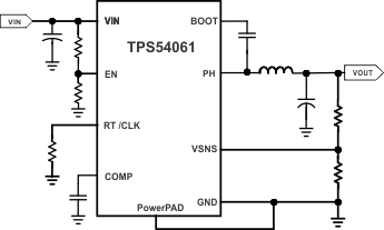
The TPS54061 device is a 60-V, 200-mA, synchronous step-down DC-DC converter with integrated high-side and low-side MOSFETs. Current mode control provides simple external compensation and flexible component selection. The non-switching supply current is 90 µA. Using the enable pin, shutdown supply current is reduced to 1.4 µA.
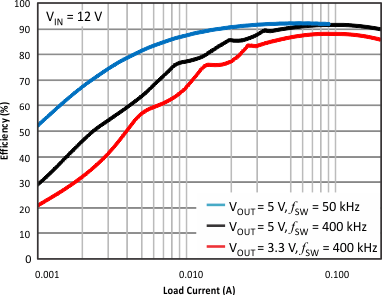
To increase light load efficiency the low-side MOSFET emulates a diode when the inductor current reaches zero.
Under voltage lockout is internally set at 4.5 V, but can be increased using two resistors on the enable pin. The output voltage startup ramp is controlled by the internal slow-start time.
The adjustable switching frequency range allows efficiency and external component size to be optimized. Frequency foldback and thermal shutdown protects the part during an overload condition.
The TPS54061 enables small designs by integrating the MOSFETs, boot recharge diode, and minimizing the IC footprint with a small 3.00 mm x 3.00 mm thermally enhanced VSON package
The TPS54061 is supported in the WEBENCH™ Designer at www.ti.com.
Device Information(1)
| PART NUMBER | PACKAGE | BODY SIZE (NOM) |
|---|---|---|
| TPS54061 | VSON (8) | 3.00 mm x 3.00 mm |
- For all available packages, see the orderable addendum at the end of the datasheet.

