-
TPS5429x 1.5-A and 2.5-A Dual, Fully-Synchronous Buck Converter With Integrated MOSFET
- 1 Features
- 2 Applications
- 3 Description
- 4 Revision History
- 5 Device Comparison Table
- 6 Pin Configuration and Functions
- 7 Specifications
-
8 Detailed Description
- 8.1 Overview
- 8.2 Functional Block Diagram
- 8.3
Feature Description
- 8.3.1 Voltage Reference
- 8.3.2 Oscillator
- 8.3.3 Input UVLO and Start-Up
- 8.3.4 Enable and Timed Turnon of the Outputs
- 8.3.5 Soft Start
- 8.3.6 Output Voltage Regulation
- 8.3.7 Inductor Selection
- 8.3.8 Maximum Output Capacitance
- 8.3.9 Feedback Loop Compensation
- 8.3.10 Bootstrap for N-Channel MOSFET
- 8.3.11 Output Overload Protection
- 8.3.12 Operating Near Maximum Duty Cycle
- 8.3.13 Dual-Supply Operation
- 8.3.14 Bypassing and Filtering
- 8.4 Device Functional Modes
-
9 Application and Implementation
- 9.1 Application Information
- 9.2
Typical Applications
- 9.2.1
TPS54291 Design Example
- 9.2.1.1 Design Requirements
- 9.2.1.2
Detailed Design Procedure
- 9.2.1.2.1 Duty Cycle Estimation
- 9.2.1.2.2 Inductor Selection
- 9.2.1.2.3 Output Capacitor Selection
- 9.2.1.2.4 Input Capacitor Selection
- 9.2.1.2.5 Feedback
- 9.2.1.2.6 Compensation Components
- 9.2.1.2.7 Compensation Gain Setting Resistor
- 9.2.1.2.8 Compensation Integrator Capacitor
- 9.2.1.2.9 Bootstrap Capacitor
- 9.2.1.2.10 Power Dissipation
- 9.2.1.3 Application Curves
- 9.2.2 TPS54290 Cascaded Design Example
- 9.2.1
TPS54291 Design Example
- 10Power Supply Recommendations
- 11Layout
- 12Device and Documentation Support
- 13Mechanical, Packaging, and Orderable Information
- IMPORTANT NOTICE
Package Options
Mechanical Data (Package|Pins)
- PWP|16
Thermal pad, mechanical data (Package|Pins)
- PWP|16
Orderable Information
TPS5429x 1.5-A and 2.5-A Dual, Fully-Synchronous Buck Converter With Integrated MOSFET
1 Features
- 4.5-V to 18-V Input Range
- Output Voltage Range 0.8 V to DMAX × VIN
- Fully Integrated Dual Buck: 1.5 A and 2.5 A
- Three Fixed Switching Frequency Versions:
- TPS54290: 300 kHz
- TPS54291: 600 kHz
- TPS54292: 1.2 MHz
- Integrated UVLO
- 0.8 VREF With 1% Accuracy (0°C to 85°C)
- Internal Soft Start:
- TPS54290: 5.2 ms
- TPS54291: 2.6 ms
- TPS54292: 1.3 ms
- Dual PWM Outputs 180° Out-of-Phase
- Dedicated Enable for Each Channel
- Current Mode Control for Simplified Compensation
- External Compensation
- Pulse-by-Pulse Overcurrent Protection,
2.2-A and 3.8-A Overcurrent Limit - Integrated Bootstrap Switch
- Thermal Shutdown Protection at 145°C
- 16-Pin PowerPAD™ HTSSOP Package
2 Applications
- Set-Top Boxes
- Digital TVs
- Power for DSP
- Consumer Electronics
3 Description
The TPS54290, TPS54291, and TPS54292 devices are dual-output, fully synchronous buck converters capable of supporting applications with a minimal number of external components. It operates from a 4.5-V to 18-V input supply voltage, and supports output voltages as low as 0.8 V and as high as 90% of the input voltage.
Both high-side and low-side MOSFETs are integrated to provide fully synchronous conversion with higher efficiency. Channel 1 can provide up to 1.5 A of continuous current. Meanwhile, Channel 2 supports up to 2.5 A.
Current mode control simplifies the compensation. The external compensation adds flexibility for the user to choose different type of output capacitors.
180° out-of-phase operation reduces the ripple current through the input capacitor, providing the benefit of reducing input capacitance, alleviating EMI and increasing capacitor life.
Device Information(1)
| PART NUMBER | PACKAGE | BODY SIZE (NOM) |
|---|---|---|
| TPS54290 TPS54291 TPS54292 |
HTSSOP (16) | 5.00 mm × 4.40 mm |
- For all available packages, see the orderable addendum at the end of the data sheet.
Simplified Schematic

4 Revision History
Changes from * Revision (October 2009) to A Revision
- Added ESD Ratings table, Thermal Information table, Feature Description section, Device Functional Modes, Application and Implementation section, Power Supply Recommendations section, Layout section, Device and Documentation Support section, and Mechanical, Packaging, and Orderable Information sectionGo
- Deleted Ordering Information table; see POA at the end of the data sheetGo
- Deleted Lead temperature (260°C maximum)Go
- Added Thermal Information table to replace the Package Dissipation Ratings tableGo
5 Device Comparison Table
| DEVICE | DESCRIPTION |
|---|---|
| TPS40222 | 5-V Input, 1.5-A, Non-Synchronous Buck Converter |
| TPS5428x | 2-A Dual Non-Synchronous Converter with Integrated High-Side FET |
| TPS5538x | 3-A Dual Non-Synchronous Converter with Integrated High-Side FET |
6 Pin Configuration and Functions
Pin Functions
| PIN | I/O | DESCRIPTION | |
|---|---|---|---|
| NO. | NAME | ||
| 1 | PVDD1 | I | Power input to the Output1 high-side MOSFET only. This pin must be locally bypassed to PGND1 with a low-ESR ceramic capacitor of 10 µF or greater. PVDD1 and PVDD2 could be tied externally together. |
| 2 | BOOT1 | I | Input supply to the high-side gate driver for Output1. Connect a 22-nF to 68-nF capacitor from this pin to SW1. This capacitor is charged from the BP pin voltage through an internal switch. The switch is turned ON during the off-time of the converter. To slow down the turn ON of the internal FET, a small resistor (2 Ω to 5 Ω) may be placed in series with the bootstrap capacitor. |
| 3 | SW1 | O | Source (switching) output for Output1 PWM |
| 4 | PGND1 | — | Power ground for Outputx. It is separated from GND to prevent the switching noise coupled to the internal logic circuits. |
| 5 | EN1 | I | Active-low enable input for Output1. If the voltage on this pin is greater than 1.5 V, Output1 is disabled (high-side switch is OFF). A voltage of less than 0.9 V enables Output1 and allow soft start of Output1 to begin. An internal current source drives this pin to PVDD2 if left floating. Connect this pin to GND to bypass the enable function. |
| 6 | EN2 | I | Active-low enable input for Output2. If the voltage on this pin is greater than 1.5 V, Output2 is disabled (high-side switch is OFF). A voltage of less than 0.9 V enables Output2 and allow soft start of Output2 to begin. An internal current source drives this pin to PVDD2 if left floating. Connect this pin to GND to bypass the enable function. |
| 7 | FB1 | I | Voltage feedback pin for Outputx. The internal transconductance error amplifier adjusts the PWM for Outputx to regulate the voltage at this pin to the internal 0.8-V reference. A series resistor divider from Outputx to ground, with the center connection tied to this pin, determines the value of the regulated output voltage. |
| 8 | COMP1 | O | Output of the transconductance (gM) amplifier. A R-C compensation network is connected from COMPx to GND. |
| 9 | COMP2 | O | Output of the transconductance (gM) amplifier. A R-C compensation network is connected from COMPx to GND. |
| 10 | FB2 | I | Voltage feedback pin for Outputx. The internal transconductance error amplifier adjusts the PWM for Outputx to regulate the voltage at this pin to the internal 0.8-V reference. A series resistor divider from Outputx to ground, with the center connection tied to this pin, determines the value of the regulated output voltage. |
| 11 | GND | — | Analog ground pin for the device. |
| 12 | BP | — | Regulated voltage to charge the bootstrap capacitors. Bypass this pin to GND with a low-ESR, 4.7-µF ceramic capacitor (10-µF capacitor preferred). |
| 13 | PGND2 | — | Power ground for Outputx. It is separated from GND to prevent the switching noise coupled to the internal logic circuits. |
| 14 | SW2 | O | Source (switching) output for Output2 PWM. |
| 15 | BOOT2 | I | Input supply to the high-side gate driver for Output2. Connect a 22-nF to 68-nF capacitor from this pin to SW2. This capacitor is charged from the BP pin voltage through an internal switch. The switch is turned ON during the off-time of the converter. To slow down the turn ON of the internal FET, a small resistor (2 Ω to 5 Ω) may be placed in series with the bootstrap capacitor. |
| 16 | PVDD2 | I | The PVDD2 pin provides power to the device control circuitry, provides the pullup for the EN1 and EN2 pins and provides power to the Output2 high-side MOSFET. This pin must be locally bypassed to PGND2 with a low-ESR ceramic capacitor of 10 µF or greater. The UVLO function monitors PVDD2 and enables the device when PVDD2 is greater than 4.2 V. |
| — | Thermal Pad | — | This pad must be tied externally to a ground plane. |
7 Specifications
7.1 Absolute Maximum Ratings
over operating free-air temperature range (unless otherwise noted)(1)| MIN | MAX | UNIT | ||
|---|---|---|---|---|
| PVDD1, PVDD2, EN1, EN2 | –0.3 | 20 | V | |
| SW1, SW2 | –1 | 20 | V | |
| BOOT1, BOOT2 | –0.3 | SW + 7 | V | |
| SW1, SW2 transient (< 50 ns) | –3 | 20 | V | |
| BP | 7 | V | ||
| FB1, FB2 | –0.3 | 3 | V | |
| Operating junction temperature, TJ | –40 | 145 | °C | |
| Storage temperature, Tstg | –55 | 155 | °C | |
7.2 ESD Ratings
| VALUE | UNIT | |||
|---|---|---|---|---|
| V(ESD) | Electrostatic discharge | Human-body model (HBM), per ANSI/ESDA/JEDEC JS-001(1) | ±2000 | V |
| Charged-device model (CDM), per JEDEC specification JESD22-C101(2) | ±1500 | |||
7.3 Recommended Operating Conditions
over operating free-air temperature range (unless otherwise noted)| MIN | MAX | UNIT | ||
|---|---|---|---|---|
| VDD | Input voltage | 4.5 | 18 | V |
| TJ | Junction temperature | –40 | 125 | °C |
7.4 Thermal Information
| THERMAL METRIC(1) | TPS54290 TPS54291 TPS54292 |
UNIT | |
|---|---|---|---|
| PWP (HTSSOP) | |||
| 16 PINS | |||
| RθJA | Junction-to-ambient thermal resistance | 39.2 | °C/W |
| RθJC(top) | Junction-to-case (top) thermal resistance | 27.7 | °C/W |
| RθJB | Junction-to-board thermal resistance | 22.3 | °C/W |
| ψJT | Junction-to-top characterization parameter | 0.8 | °C/W |
| ψJB | Junction-to-board characterization parameter | 22.1 | °C/W |
| RθJC(bot) | Junction-to-case (bottom) thermal resistance | 2.7 | °C/W |
7.5 Electrical Characteristics
TJ = –40°C to 125°C, PVDD1 and PVDD2 = 12 V (unless otherwise noted)| PARAMETER | TEST CONDITIONS | MIN | TYP | MAX | UNIT | ||
|---|---|---|---|---|---|---|---|
| INPUT SUPPLY | |||||||
| PVDD1, PVDD2 | Input voltage range | 4.5 | 18 | V | |||
| IDDSDN | Shutdown current | EN1 = EN2 = PVDD2 (4.5 V to 18 V) | 80 | 160 | µA | ||
| IDDQ | Quiescent, non-switching | FB1 = FB2 = 1 V, outputs off | 1.65 | 3 | mA | ||
| IDDSW | Quiescent, while switching | FB1 = FB2 = 0.75 V, measured at BP | 10 | mA | |||
| UVLO | Minimum turnon voltage | PVDD2 only | 3.8 | 4.1 | 4.4 | V | |
| UVLOHYS | Hysteresis | 460 | 600 | mV | |||
| tstart(1)(2) | Time from start-up to soft start begin | CBP = 10 µF, EN1 and EN2 go low simultaneously | 1.5 | ms | |||
| ENABLE (ACTIVE LOW) | |||||||
| VENx | Enable threshold voltage | 0.9 | 1.2 | 1.5 | V | ||
| Hysteresis | 70 | mV | |||||
| IENx | Enable pullup current | 10 | µA | ||||
| tENx(1) | Time from enable to soft start begin | Other enable pin = GND | 10 | µs | |||
| BP REGULATOR | |||||||
| BP | Regulator voltage | 8 V ≤ VPVDD2 ≤ 18 V | 5 | 5.2 | 5.6 | V | |
| BPLDO | Dropout voltage | VPVDD2 = 4.5 V | 400 | mV | |||
| IBPS | Regulator short current | 4.5 V ≤ VPVDD2 ≤ 18 V | 25 | mA | |||
| OSCILLATOR | |||||||
| fSW | Oscillator frequency | TPS54290 | 260 | 300 | 360 | kHz | |
| TPS54291 | 520 | 600 | 720 | ||||
| TPS54292 | 1040 | 1200 | 1440 | kHz | |||
| tDEAD(1) | Clock dead time | 140 | ns | ||||
| gMTRANSCONDUCTANCE AMPLIFIER AND VOLTAGE REFERENCE (APPLIES TO BOTH CHANNELS) | |||||||
| VFB | Feedback input voltage | 0°C < TJ < 85°C | 792 | 800 | 808 | mV | |
| –40ºC < TJ < 125°C | 786 | 800 | 812 | mV | |||
| IFB | Feedback Input bias current | VFB = 0.8 V | 5 | 50 | nA | ||
| gM(1) | Transconductance | 200 | 325 | 450 | µS | ||
| ISOURCE | Error amplifier source current capability | VFB1 = VFB2 = 0.7 V, VCOMP = 0 V | 15 | 30 | 40 | µA | |
| ISINK | Error amplifier sink current capability | VFB1 = VFB2 = 0.9 V, VCOMP = 2 V | 15 | 30 | 40 | µA | |
| SOFT START (APPLIES TO BOTH CHANNELS) | |||||||
| tSS | Soft-start time | TPS54290, 0 V ≤ VFB ≤ 0.8 V | 4 | 5.2 | 6 | ms | |
| TPS54291 | 2 | 2.6 | 3 | ||||
| TPS54292 | 1 | 1.3 | 1.6 | ||||
| OVERCURRENT PROTECTION | |||||||
| ICL1 | Current limit CH1 | 1.8 | 2.2 | 2.6 | A | ||
| ICL2 | Current limit CH2 | 3.2 | 3.8 | 4.6 | A | ||
| THICCUP(1) | Hiccup timeout | TPS54290 | 30 | ms | |||
| TPS54291 | 16 | ||||||
| TPS54292 | 8 | ||||||
| tONOC(1) | Minimum overcurrent pulse | 150 | 200 | ns | |||
| BOOTSTRAP (APPLIED TO BOTH CHANNELS) | |||||||
| RBOOT | Bootstrap switch resistance | R(BP to BOOT), I external = 10 mA | 33 | Ω | |||
| PGOOD | |||||||
| VUV | Feedback voltage limit for PGOOD | 660 | 730 | mV | |||
| VPG-HYST(1) | PGOOD hysteresis voltage on FB | 40 | mV | ||||
| OUTPUT STAGE (APPLIED TO BOTH CHANNELS) | |||||||
| RDS(on1)(HS)(1) | On-resistance of high-side FET and bondwire on CH1 | 170 | 265 | mΩ | |||
| RDS(on2)(HS)(1) | On-resistance of high-side FET and bondwire on CH2 | 120 | 190 | mΩ | |||
| RDS(on1)(LS)(1) | On-resistance of low-side FET and bondwire on CH1 | 120 | 190 | mΩ | |||
| RDS(on2)(LS)(1) | On-resistance of low-side FET and bondwire on CH2 | 90 | 150 | mΩ | |||
| tON_MIN (1) | Minimum controllable pulse width | 150 | ns | ||||
| Minimum duty cycle | VFB = 0.9 V | 0% | |||||
| tDEAD(1) | Output driver dead time | HDRV off to LDRV on | 20 | ns | |||
| LDRV off to HDRV on | 20 | ns | |||||
| DMAX | Maximum duty cycle | TPS54290 | 90% | 96% | |||
| TPS54291 | 85% | 91% | |||||
| TPS54292 | 78% | 82% | |||||
| THERMAL SHUTDOWN | |||||||
| TSD(1) | Shutdown temperature | 145 | °C | ||||
| TSD_HYS(1) | Hysteresis | 20 | °C | ||||
7.6 Typical Characteristics
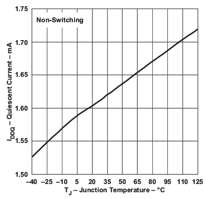 Figure 1. Quiescent Current vs Temperature
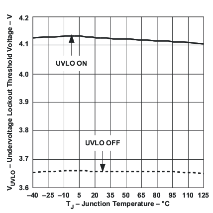 Figure 3. UVLO Turnon and Turnoff Thresholds
vs Temperature
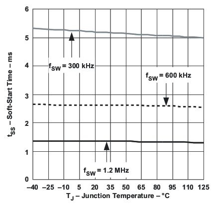 Figure 5. Soft-Start Time vs Temperature
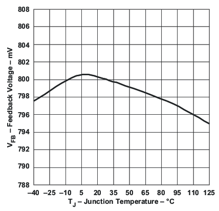 Figure 7. Feedback Voltage vs Temperature
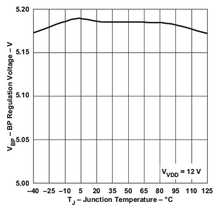 Figure 9. BP Voltage vs Temperature
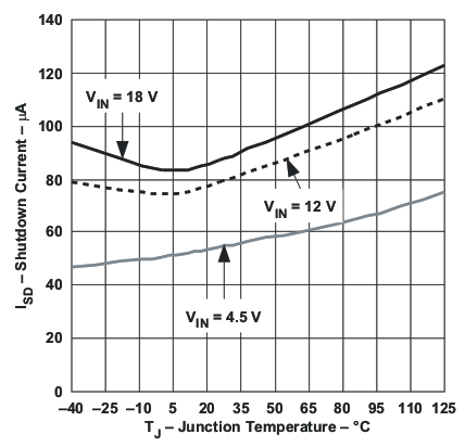 Figure 2. Shutdown Current vs Temperature
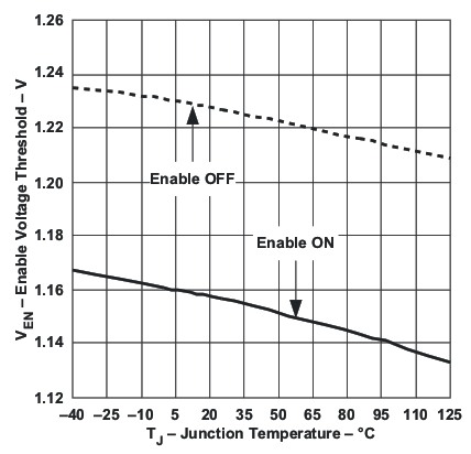 Figure 4. ENx Turnon and Turnoff Threshold
vs Temperature
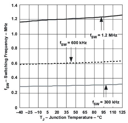 Figure 6. Oscillator Frequency vs Temperature
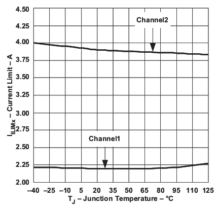 Figure 8. Current Limit vs Temperature
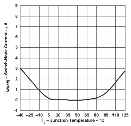 Figure 10. SW Node Leakage Current
vs Temperature
8 Detailed Description
8.1 Overview
The TPS5429x is a dual-output fully synchronous buck converter. Each PWM channel contains an error amplifier, current mode pulse width modulator (PWM), switching and rectifying MOSFETs, enable, and fault protection circuitry. Common to the two channels are the internal voltage regulator, voltage reference, and clock oscillator.
8.2 Functional Block Diagram

8.3 Feature Description
8.3.1 Voltage Reference
The band-gap cell common to both outputs, trimmed to 800 mV. The reference voltage is 1% accurate in the temperature range from 0°C to 85°C.
8.3.2 Oscillator
The oscillator frequency is internally fixed at 2.4 MHz that is divided by 8/4/2 to generate the ramps for TPS5429x, respectively. The two outputs are internally configured to operate on alternating switch cycles (that is, 180° out-of-phase).
8.3.3 Input UVLO and Start-Up
When the voltage at the PVDD2 pin is less than 4.4 V, a portion of the internal bias circuitry is operational, and all other functions are held OFF. All of the internal MOSFETs are also held OFF. When the PVDD2 voltage rises above the UVLO turnon threshold, the state of the enable pins determines the remainder of the internal start-up sequence. If either output is enabled (ENx pulled low), the BP regulator turns on, charging the BP capacitor with a 20-mA current. When the BP pin is greater than 4 V, PWM is enabled and soft start commences.
NOTE
The internal regulator and control circuitry are powered from PVDD2. The voltage on PVDD1 may be higher or lower than PVDD2.
8.3.4 Enable and Timed Turnon of the Outputs
Each output has a dedicated (active low) enable pin. If left floating, an internal current source pulls the pin to PVDD2. By grounding, or by pulling the ENx pin to below approximately 1.25 V with an external circuit, the associated output is enabled and soft start is initiated.
If both enable pins are left in the high state, the device operates in a shutdown mode, where the BP regulator shuts down and minimal house keeping functions are active. The total standby current from both PVDD pins is 80 µA at 12-V input supply.
An R-C connect to an ENx pin may be used to delay the turnon of the associated output after power is applied to PVDDx (see Figure 11). After power is applied to PVDD2, the voltage on the ENx pin slowly decays towards ground. Once the voltage decays to approximately 1.25 V, then the output is enabled and the start-up sequence begins. If it is desired to enable the outputs of the device immediately upon the application of power to the PVDD2 pin, then omit these two components and tie the ENx pin to GND directly.
If an R-C circuit is used to delay the turnon of the output, the resistor value must be an order of magnitude less than 1.25 V / 10 µA or 120 kΩ. A suggested value is 51 kΩ. This allows the ENx voltage to decay below the 1.25-V threshold while the 10-µA bias current flows.
The time to start (after the application of PVDD2) is Equation 1.

where
- R and C are the timing components
- VTH is the 1.25-V enable threshold voltage
- IEN is the 10-µA maximum enable pin biasing current
Figure 11 and Figure 12 illustrate startup delay with an R-C filter on the enable pin(s).
 Figure 11. Start-Up Delay Schematic
 Figure 12. Start-Up Delay Timing Diagram
NOTE
If delayed output voltage start-up is not necessary, simply connect EN1 and EN2 to GND. This allows the outputs to start immediately on the valid application of PVDD2.
If ENx is allowed to go high after the Outputx has been in regulation, the upper and lower MOSFETs shut off, and the output decays at a rate determined by the output capacitor and the load.
8.3.5 Soft Start
Each output has a dedicated soft-start circuit. The soft-start voltage is an internal digital reference ramp to one of the two noninverting inputs of the error amplifier. The other input is the internal precise 0.8-V reference. The total ramp time for the FB voltage to charge from 0 V to 0.8 V is about 5.2 ms, 2.6 ms, and 1.3 ms for TPS54190, TPS54191, and TPS54192, respectively. During a soft-start interval, the TPS5429x output slowly increases the voltage to the noninverting input of the error amplifier. In this way, the output voltage slowly ramps up until the voltage on the noninverting input to the error amplifier reaches the internal 0.8-V reference voltage. At that time, the voltage at the noninverting input to the error amplifier remains at the reference voltage.
During the soft-start interval, pulse-by-pulse current limiting is in effect. If an overcurrent pulse is detected, six PWM pulses is skipped to allow the inductor current to decay before another PWM pulse is applied (see Output Overload Protection). There is no pulse skipping if a current limit pulse is not detected.
If the rate of rise of the input voltage (PVDDx) is such that the input voltage is too low to support the desired regulation voltage by the time soft start completes, the output UV circuit may trip and cause a hiccup in the output voltage. In this case, use a timed delay start-up from the ENx pin to delay the start-up of the output until the PVDDx voltage has the capability of supporting the desired regulation voltage.
8.3.6 Output Voltage Regulation
The regulation output voltage is determined by a resistor divider connecting the output node, the FBx pin, and GND (Figure 13). The value of the output voltage is shown in Equation 2.

where
- VREF is the internal 0.8-V reference voltage
 Figure 13. Feedback Network for Channel 1
8.3.7 Inductor Selection
Equation 3 calculates the inductance value so that the output ripple current falls from 20% to 40% of the full load current.

8.3.8 Maximum Output Capacitance
With internal pulse-by-pulse current limiting and a fixed soft-start time, there is a maximum output capacitance which may be used before start-up problems begin to occur. If the output capacitance is large enough so that the device enters a current-limit protection mode during start-up, then there is a possibility that the output never reaches regulation. Instead, the TPS5429x simply shuts down and attempts a restart as if the output were short-circuited to ground. The maximum output capacitance (including bypass capacitance distributed at the load) is given by Equation 4.

where
- tSS is the soft-start time
- ILIM is the current limit level
8.3.9 Feedback Loop Compensation
In the feedback signal path, the output voltage setting divider is followed by an internal gM-type error amplifier with a typical transconductance of 325 µS. An external series connected R-C circuit from the gM amplifier output (COMPx pin) to ground serves as the compensation network for the converter. The signal from the error amplifier output is then buffered and combined with a slope compensation signal before it is mirrored to be referenced to the SW node. Here, it is compared with the current feedback signal to create a pulse-width-modulated (PWM) signal-fed to drive the upper MOSFET switch. A simplified equivalent circuit of the signal control path is depicted in Figure 14.
NOTE
Noise coupling from the SWx node to internal circuitry of BOOTx may impact narrow pulse width operation, especially at load currents less than 1 A.
 Figure 14. Feedback Loop Equivalent Circuit
A more conventional small-signal equivalent block diagram is shown in Figure 15. Here, the full closed-loop signal path is shown. Because the TPS5429x contains internal slope compensation, the external L-C filter must be selected appropriately so that the resulting control loop meets criteria for stability.
 Figure 15. Small Signal Equivalent Block Diagram
To determine the components necessary for compensating the feedback loop, the controller frequency response characteristics must be understood and the desired crossover frequency selected. The best results are obtained if 10% of the switching frequency is used as this closed-loop crossover frequency. In some cases, up to 20% of the switching frequency is also possible.
With the output filter components selected, the next step is to calculate the DC gain of the modulator. For TPS5429x, use Equation 5.

where
- K = 5.6 ×10⁵ for TPS54290
- K = 1.5 × 10⁶ for TPS54291
- K = 3.6 × 10⁶ for TPS54292
The overall DC gain of the converter control-to-output transfer function is approximated by Equation 6.

The next step is to find the desired gain of the error amplifier at the desired crossover frequency. Assuming a single-pole roll-off, use Equation 6 to evaluate Equation 7 at the desired crossover frequency.

where
- ƒCO is the desired crossover frequency
 Figure 16. Loop Compensation Network
If operating at wide duty cycles (over 50%), a capacitor may be necessary across the upper resistor of the voltage setting divider (see Equation 8). If duty cycles are less than 50%, this capacitor may be omitted.

If a high-ESR capacitor is used in the output filter, a zero appears in the loop response that could lead to instability (see Equation 9). To compensate, a small capacitor is placed in parallel with the lower voltage setting divider resistor. The value of the capacitor is determined such that a pole is placed at the same frequency as the ESR zero. If low-ESR capacitors are used, this capacitor may be omitted.

Next, calculate the value of the error amplifier gain setting resistor and capacitor using Equation 10 and Equation 11.


where
NOTE
When the filter and compensation component values have been established, laboratory measurements of the physical design must be performed to confirm converter stability.
8.3.10 Bootstrap for N-Channel MOSFET
A bootstrap circuit provides a voltage source higher than the input voltage and of sufficient energy to fully enhance the switching MOSFET each switching cycle. The PWM duty cycle is limited to maximum (that is, 90% for TPS54291) allowing an external bootstrap capacitor to charge through an internal synchronous switch (between BP and BOOTx) during every cycle. When the PWM switch is commanded to turn on, the energy used to drive the MOSFET gate is derived from the voltage on this capacitor.
Because this is a charge transfer circuit, take care in selecting the value of the bootstrap capacitor. It must be sized such that the energy stored in the capacitor on a per cycle basis is greater than the gate charge requirement of the MOSFET being used. Typically a ceramic capacitor with a value from 22 nF to 68 nF is selected for the bootstrap capacitor.
8.3.11 Output Overload Protection
In the event of an overcurrent on either output after the output reaches regulation, pulse-by-pulse current limit is in effect for that output. In addition, an output undervoltage (UV) comparator monitors the FBx voltage (which follows the output voltage) to declare a fault if the output drops below 85% of regulation. During this fault condition, both PWM outputs are disabled. This ensures that both outputs discharge to GND, in the event that overcurrent is on one output while the other is not loaded. The converter enters a hiccup mode timeout before attempting to restart.
If an overcurrent condition exists during soft start, pulse-by-pulse current limiting reduces the pulse width of the affected output’s PWM. In addition, if an overcurrent pulse is detected, six clock cycles are skipped before a next PWM pulse is enabled, effectively dividing the PWM frequency by six and preventing excessive current build up in the inductor. At the end of the soft-start time, a UV fault is declared and the operation is the same as described above.
The overcurrent threshold for Output1 and Output2 are set nominally 2.2 A and 3.8 A, respectively.
NOTE
Design hint: The OCP Threshold refers to the peak current in the internal switch. Be sure to add the 1/2 of the peak inductor ripple current to the DC load current in determining how close the actual operating point is to the OCP Threshold.
8.3.12 Operating Near Maximum Duty Cycle
If the TPS5429x is operated at maximum duty cycle, and if the input voltage is insufficient to support the output voltage (at full load or during a load current transient) then there is a possibility that the output voltage falls from regulation and trip the output UV comparator. If this must occur, the TPS5429x protection circuitry declares a fault and enters hiccup mode.
NOTE
Design hint: Ensure that under ALL conditions of line and load regulation that there is sufficient duty cycle to maintain output voltage regulation.
8.3.13 Dual-Supply Operation
It is possible to operate a TPS5429x from two supply voltages. If this application is desired, then the sequencing of the supplies must be such that PVDD2 is above the UVLO voltage before PVDD1 begins to rise. This is to ensure the internal regulator and the control circuitry is in operation before PVDD1 supplies energy to the output. In addition, Output1 must be held in the disabled state (EN1 high) until there is sufficient voltage on PVDD1 to support Output1 in regulation (see Operating Near Maximum Duty Cycle).
The preferred sequence of events follows:
- PVDD2 rises above the input UVLO voltage
- PVDD1 rises with Output1 disabled until PVDD1 rises above level to support Output1 regulation
With the two conditions above satisfied, there is no restriction on PVDD2 to be greater than, or less than PVDD1.
NOTE
Design hint: An R-C delay on EN1 may be used to delay the start-up of Output1 for a long enough period of time to ensure PVDD1 can support Output1 load.
8.3.14 Bypassing and Filtering
As with any integrated circuit, supply bypassing is important for jitter-free operation. To improve the noise immunity of the converter, ceramic bypass capacitors must be placed as close to the package as possible.
- PVDD1 to GND: Use a 10-µF ceramic capacitor
- PVDD2 to GND: Use a 10-µF ceramic capacitor
- BP to GND: Use a 4.7-µF ceramic capacitor
8.4 Device Functional Modes
8.4.1 PWM Operation
TPS5429X is a dual-channel synchronous buck converter. Normal operation occurs when VIN is above 4.5 V and the EN1 and EN2 pins pulled low to enable the device.
8.4.2 Standby Operation
TPS5429X can be placed in standby when the EN1 and EN2 pins are set high, disabling the device.
9 Application and Implementation
NOTE
Information in the following applications sections is not part of the TI component specification, and TI does not warrant its accuracy or completeness. TI’s customers are responsible for determining suitability of components for their purposes. Customers should validate and test their design implementation to confirm system functionality.
9.1 Application Information
TPS5429X is a synchronous buck converter. It can convert an input voltage of 4.5 V to 18 V to two lower voltages. Channel 1 is rated for 1.5-A output, while Channel 2 is rated for 2.5-A output.
9.2 Typical Applications
9.2.1 TPS54291 Design Example
The following example illustrates the design process and component selection for a 12-V to 5-V or 3.3-V dual non-synchronous buck regulator using the TPS54291 converter.
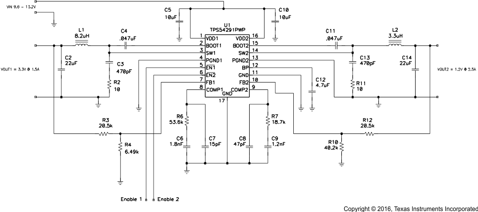 Figure 17. TPS54291 Design Example 1 Schematic
9.2.1.1 Design Requirements
A definition of symbols used can be found in Table 1. The efficiency, line regulation, and load regulation from printed-circuit boards built using this design are shown in Figure 19 and Figure 20.
Table 1. Design Example Electrical Characteristics
| PARAMETER | TEST CONDITIONS | MIN | TYP | MAX | UNIT | ||
|---|---|---|---|---|---|---|---|
| INPUT CHARACTERISTICS | |||||||
| VIN | Input voltage | 8 | 12 | 14 | V | ||
| IIN | Input current | VIN = nom, IOUT = max | A | ||||
| No load input current | VIN = nom, IOUT = 0 A | 12 | 20 | mA | |||
| VIN(UVLO) | Input UVLO | IOUT = min to max | 4 | 4.2 | 4.4 | V | |
| OUTPUT CHARACTERISTICS | |||||||
| VOUT1 | Output voltage 1 | VIN = nom, IOUT = nom | 3.2 | 3.3 | 3.4 | V | |
| VOUT2 | Output voltage 2 | VIN = nom, IOUT = nom | 1.15 | 1.2 | 1.25 | V | |
| Line regulation | VIN = min to max | 1% | |||||
| Load regulation | IOUT = min to max | 1% | |||||
| VOUT1(ripple) | Output1 voltage ripple | VIN = nom, IOUT1 = max | 50 | mVPP | |||
| VOUT2(ripple) | Output2 voltage ripple | VIN = nom, IOUT2 = max | 24 | mVPP | |||
| IOUT1 | Output current 1 | VIN = min to max | 0 | 1.5 | A | ||
| IOUT2 | Output current 2 | VIN = min to max | 0 | 2.5 | A | ||
| IOCP1 | Output overcurrent Channel 1 | VIN = nom, VOUT = (VOUT1 – 5%) | 1.8 | 2.2 | 2.6 | A | |
| IOCP2 | Output overcurrent Channel 2 | VIN = nom, VOUT = (VOUT2 – 5%) | 3.2 | 3.8 | 4.6 | A | |
| TRANSIENT RESPONSE | |||||||
| ΔVOUT | Change from load transient | ΔIOUT = 1 A at 3 µA/s | 200 | mV | |||
| Settling time | to 1% of VOUT | 1 | ms | ||||
| SYSTEMS CHARACTERISTICS | |||||||
| fSW | Switching frequency | 500 | 600 | 700 | kHz | ||
| ηPEAK | Peak efficiency | VIN = nom | 90% | ||||
| η | Full load efficiency | VIN = nom, IOUT = max | 80% | ||||
| TOP | Operating temperature | VIN = min to max, IOUT = min to max | 0 | 25 | 60 | °C | |
9.2.1.2 Detailed Design Procedure
The list of materials for this application is shown below in Table 2.
Table 2. Design Example List of Materials
| REFERENCE DESIGNATOR |
QTY | VALUE | DESCRIPTION | SIZE | PART NUMBER | MFR |
| C12 | 1 | 4.7 µF | Capacitor, Ceramic, 10 V, X5R, 20% | 0805 | Std | Std |
| C2, C14 | 2 | 22 µF | Capacitor, Ceramic, 6.3 V, X5R, 20% | 1206 | C3216X5R0J226M | TDK |
| C3, C13 | 2 | 470 pF | Capacitor, Ceramic, 25 V, X7R, 20% | 0603 | Std | Std |
| C4, C11 | 2 | 0.047 µF | Capacitor, Ceramic, 25 V, X7R, 20% | 0603 | Std | Std |
| C5, C10 | 2 | 10 µF | Capacitor, Ceramic, 25 V, X5R, 20% | 1210 | C3225X5R1E106M | TDK |
| C6 | 2 | 1.8 nF | Capacitor, Ceramic, 25 V, X7R, 20% | 0603 | Std | Std |
| C7 | 1 | 15 pF | Capacitor, Ceramic, 25 V, X7R, 20% | 0603 | Std | Std |
| C8 | 1 | 47 pF | Capacitor, Ceramic, 25 V, X7R, 20% | 0603 | Std | Std |
| C9 | 1 | 1.2 nF | Capacitor, Ceramic, 25 V, X7R, 20% | 0603 | Std | Std |
| L1 | 1 | 8.2 µH | Inductor, SMT, 4.38 A, 20 mΩ | 0.402 × 0.394 inch | MSS1048-822L | Coilcraft |
| L2 | 1 | 3.3 µH | Inductor, SMT, 5.04 A, 10 mΩ | 0.402 × 0.394 inch | MSS1048-332L | Coilcraft |
| R10 | 1 | 40.2 kΩ | Resistor, Chip, 1/16W, 1% | 0603 | Std | Std |
| R2, R11 | 2 | 10 Ω | Resistor, Chip, 1/16W, 5% | 0603 | Std | Std |
| R3, R12 | 2 | 20.5 kΩ | Resistor, Chip, 1/16W, 1% | 0603 | Std | Std |
| R4 | 1 | 6.49 kΩ | Resistor, Chip, 1/16W, 1% | 0603 | Std | Std |
| R6 | 1 | 7.87 kΩ | Resistor, Chip, 1/16W, 1% | 0603 | Std | Std |
| R7 | 1 | 4.64 kΩ | Resistor, Chip, 1/16W, 1% | 0603 | Std | Std |
| U1 | 1 | 2.5 A/1.5 A, 600 Hz | Dual Output Fully Synchronous Buck Converter w/Integrated FET | CSP | TPS54291PWP | TI |
9.2.1.2.1 Duty Cycle Estimation
The duty cycle of the main switching FET is estimated by Equation 12 and Equation 13.


9.2.1.2.2 Inductor Selection
The peak-to-peak ripple must be limited to between 20% and 30% of the maximum output current (see Equation 14 and Equation 15).


The minimum inductor size can be estimated by Equation 16 and Equation 17.


The standard inductor values of 8.2 µH and 3.3 µH are selected for Channel 1 and Channel 2, respectively. The actual ripple currents are estimated by Equation 18 and Equation 19.


The RMS current through the inductor is approximated by Equation 20 and Equation 21.


A DC current with 30% peak-to-peak ripple has an RMS current approximately 0.4% above the average current.
The peak inductor current is estimated by Equation 22 and Equation 23.


A 8.2-µH inductor with a minimum RMS current rating of 1.51 A and minimum saturation current rating of 3.7 A must be selected. A Coilcraft MSS1048-822ML 8.2-µH, 4.38-A inductor is chosen for Channel 1 and a Coilcraft MSS1048-332 3.3-µH inductor is chosen for Channel 2.
9.2.1.2.3 Output Capacitor Selection
Output capacitors are selected to support load transients and output ripple current. The minimum output capacitance to meet the transient specification is given by Equation 24 and Equation 25.


The maximum ESR to meet the ripple specification is given by Equation 26 and Equation 27.


A single 22-µF ceramic capacitor with approximately 2.5 mΩ of ESR is selected to provide sufficient margin for capacitance loss due to DC voltage bias.
9.2.1.2.4 Input Capacitor Selection
A minimum 10-µF ceramic input capacitor on each PVDD pin is recommended. The ceramic capacitor must handle the RMS ripple current in the input capacitor.
The RMS current in the input capacitors is estimated by Equation 28 and Equation 29.


One 1210 10-µF, 25-V, X5R, ceramic capacitor with 2-mΩ ESR and a 2-A RMS current rating are selected for each PVDD input. Higher voltage capacitors are selected to minimize capacitance loss at the DC bias voltage to ensure the capacitors have sufficient capacitance at the working voltage.
9.2.1.2.5 Feedback
The primary feedback divider resistor (RFB) from VOUT to FB must be selected between 10-kΩ and 100-kΩ to maintain a balance between power dissipation and noise sensitivity. For a 3.3-V and 5-V output, 20.5 kΩ is selected and the lower resistor is given by Equation 30.

For RFB = 20.5 kΩ and VFB = 0.8 V, RBIAS = 6.56 kΩ and 41.0 kΩ (6.49 kΩ and 40.2 kΩ selected) for 3.3 V and 1.2 V, respectively. It is common to select the next lower available resistor value for the bias resistor. This biases the nominal output voltage slightly higher, allowing additional tolerance for load regulation.
9.2.1.2.6 Compensation Components
The TPS54291 controller uses a transconductance error amplifier, which is compensated with a series capacitor and resistor to ground plus a high-frequency capacitor to reduce the gain at high frequency. To select the component, Equation 31 to Equation 33 define the control loop and power stage gain and transfer function.

where
- K = 5.6 × 10⁵ for TPS54290
- K = 1.5 × 10⁶ for TPS54291
- K = 3.6 × 10⁶ for TPS54292
The overall DC gain of the converter control-to-output transfer function is approximated by Equation 32.

With the power stage DC gain, it is possible to estimate the required mid-band gain to program a desired crossover frequency.

9.2.1.2.7 Compensation Gain Setting Resistor
RCOMP programs the mid-band error amplifier gain to set the desired crossover frequency in Equation 34.

9.2.1.2.8 Compensation Integrator Capacitor
An integrator capacitor provides maximum DC gain for the best possible DC regulation while programming the compensation zero to match the natural pole of the output filter (see Equation 35). CCOMP is selected by Equation 36.


9.2.1.2.9 Bootstrap Capacitor
To ensure proper charging of the high-side FET gate and limit the ripple voltage on the boost capacitor, a 47-nF boot strap capacitor is recommended.
9.2.1.2.10 Power Dissipation
The power dissipation in the TPS54291 is made from FET conduction losses, switching losses and regulator losses.
Conduction losses are estimated by Equation 37 and Equation 38.


The switching losses are estimated by Equation 39 and Equation 40.


The regulator losses are estimated by Equation 41.

Total power dissipation in the device is the sum of conduction losses and switching losses for both channels plus regulator losses, which is estimated to be 1.01 W.
9.2.1.3 Application Curves
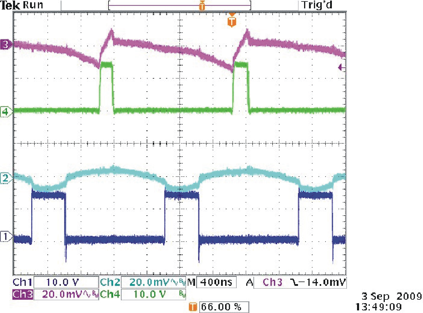 Figure 18. TPS54291 Design Example
Switching Waveforms
 Figure 20. Design Efficiency for 3.3-V Output
 Figure 19. Design Efficiency for 1.2-V Output
9.2.2 TPS54290 Cascaded Design Example
TPS5429x can be configured as cascaded operation as shown in Figure 21. The 12-V input supply is applied to PVDD2 and the Channel 2 output is tied to PVDD1. The Channel 2 output is 3.3 V and capable of supporting 1.5 A to the load while generating power for the 1.2-V input for Channel 1.
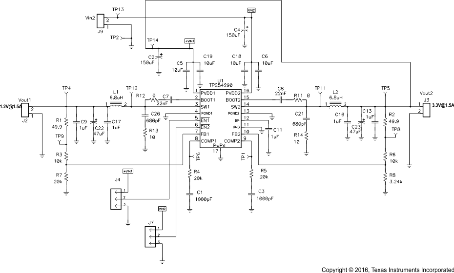 Figure 21. Cascading Operation
9.2.2.1 Application Curves
For Figure 22: Channel 1 is a 12-V supply, Channel 2 is VOUT1 (1.2 V), and Channel 3 is VOUT2(3.3 V).
For Figure 23: Channel 1 is Channel 1 SW node and Channel 2 is Channel 1 output ripple; Channel 3 is Channel 2 output ripple and Channel 2 is Channel 2 SW node.
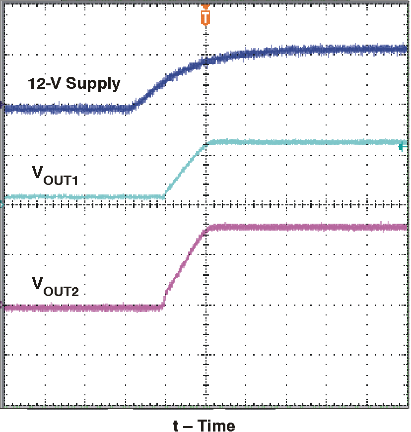 Figure 22. Start-Up Waveforms
 Figure 23. Output Ripple and SW Nodes
