TPS54560-Q1 4.5-V to 60-V Input, 5-A, Step-Down DC-DC Converter With Eco-Mode™
1 Features
- Qualified for Automotive Applications
- AEC-Q100 Qualified With the Following Results:
- Device Temperature Grade 1: –40°C to 125°C Ambient Operating Temperature Range
- Device HBM ESD Classification Level H1C
- Device CDM ESD Classification Level C3B
- High Efficiency at Light Loads With Pulse-Skipping Eco-Mode™
- 92-mΩ High-Side MOSFET
- 146-μA Operating Quiescent Current and 2-µA Shutdown Current
- 100-kHz to 2.5-MHz Adjustable Switching Frequency
- Synchronizes to External Clock
- Low Dropout at Light Loads with Integrated BOOT Recharge FET
- Adjustable UVLO Voltage and Hysteresis
- 0.8-V 1% Internal Voltage Reference
- 8-Pin HSOIC with PowerPAD™ Package
- –40°C to 150°C TJOperating Range
- Supported by WEBENCH® Software Tool
2 Applications
3 Description
The TPS54560-Q1 is a 60-V, 5-A, step-down regulator with an integrated high side MOSFET. The device survives load dump pulses up to 65 V per ISO 7637. Current mode control provides simple external compensation and flexible component selection. A low-ripple, pulse-skip mode reduces the no load supply current to 146 μA. Shutdown supply current is reduced to 2 μA when the enable pin is pulled low.
Undervoltage lockout is internally set at 4.3 V but can be increased using an external resistor divider at the enable pin. The output voltage start-up ramp is internally controlled to provide a controlled start-up and eliminate overshoot.
A wide adjustable frequency range allows either efficiency or external component size to be optimized. Output current is limited cycle-by-cycle. Frequency foldback and thermal shutdown protects internal and external components during an overload condition.
The TPS54560-Q1 is available in an 8-pin thermally enhanced HSOIC PowerPAD package.
Device Information(1)
| PART NUMBER | PACKAGE | BODY SIZE (NOM) |
|---|---|---|
| TPS54560-Q1 | SO PowerPAD (8) | 3.90 mm x 4.89 mm |
- For all available packages, see the orderable addendum at the end of the datasheet.
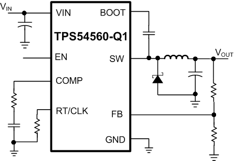
Simplified Schematic
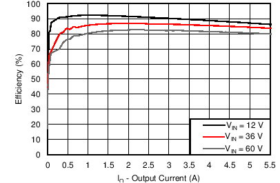
Efficiency vs Load Current
4 Revision History
Changes from * Revision (September 2013) to A Revision
- Added ESD Ratings table, Feature Description section, Device Functional Modes, Application and Implementation section, Power Supply Recommendations section, Layout section, Device and Documentation Support section, and Mechanical, Packaging, and Orderable Information section.Go
5 Pin Configuration and Functions
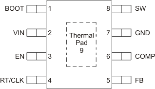
Pin Functions
| PIN | I/O | DESCRIPTION | ||
|---|---|---|---|---|
| NAME | NO. | |||
| BOOT | 1 | O | A bootstrap capacitor is required between BOOT and SW. If the voltage on this capacitor is below the minimum required to operate the high-side MOSFET, the output is switched off until the capacitor is refreshed. | |
| VIN | 2 | I | Input supply voltage with 4.5 V to 60 V operating range. | |
| EN | 3 | I | Enable pin, with internal pull-up current source. Pull below 1.2 V to disable. Float to enable. Adjust the input undervoltage lockout with two resistors. See the Enable and Adjusting Undervoltage Lockout section. | |
| RT/CLK | 4 | I | Resistor Timing and External Clock. An internal amplifier holds this pin at a fixed voltage when using an external resistor to ground to set the switching frequency. If the pin is pulled above the PLL upper threshold, a mode change occurs and the pin becomes a synchronization input. The internal amplifier is disabled and the pin is a high impedance clock input to the internal PLL. If clocking edges stop, the internal amplifier is re-enabled and the operating mode returns to resistor frequency programming. | |
| FB | 5 | I | Inverting input of the transconductance (gm) error amplifier. | |
| COMP | 6 | O | Error amplifier output and input to the output switch current (PWM) comparator. Connect frequency compensation components to this pin. | |
| GND | 7 | – | Ground | |
| SW | 8 | I | The source of the internal high-side power MOSFET and switching node of the converter. | |
| Thermal Pad | 9 | – | GND pin must be electrically connected to the exposed pad on the printed circuit board for proper operation. | |