-
TPS54620 4.5-V to 17-V Input, 6-A, Synchronous, Step-Down SWIFT™ Converter
- 1 Features
- 2 Applications
- 3 Description
- 4 Revision History
- 5 Pin Configurations and Functions
- 6 Specifications
-
7 Detailed Description
- 7.1 Overview
- 7.2 Functional Block Diagram
- 7.3
Feature Description
- 7.3.1 Fixed Frequency PWM Control
- 7.3.2 Continuous Current Mode Operation (CCM)
- 7.3.3 VIN and Power VIN Pins (VIN and PVIN)
- 7.3.4 Voltage Reference
- 7.3.5 Adjusting the Output Voltage
- 7.3.6 Safe Start-Up into Prebiased Outputs
- 7.3.7 Error Amplifier
- 7.3.8 Slope Compensation
- 7.3.9 Enable and Adjusting Undervoltage Lockout
- 7.3.10 Adjustable Switching Frequency and Synchronization (RT/CLK)
- 7.3.11 Slow Start (SS/TR)
- 7.3.12 Power Good (PWRGD)
- 7.3.13 Output Overvoltage Protection (OVP)
- 7.3.14 Overcurrent Protection
- 7.3.15 Thermal Shutdown
- 7.3.16 Small Signal Model for Loop Response
- 7.3.17 Simple Small Signal Model for Peak Current Mode Control
- 7.3.18 Small Signal Model for Frequency Compensation
- 7.4 Device Functional Modes
-
8 Application and Implementation
- 8.1 Application Information
- 8.2
Typical Application
- 8.2.1 Design Requirements
- 8.2.2
Detailed Design Procedures
- 8.2.2.1 Custom Design With WEBENCH Tools
- 8.2.2.2 Operating Frequency
- 8.2.2.3 Output Inductor Selection
- 8.2.2.4 Output Capacitor Selection
- 8.2.2.5 Input Capacitor Selection
- 8.2.2.6 Slow-Start Capacitor Selection
- 8.2.2.7 Bootstrap Capacitor Selection
- 8.2.2.8 Undervoltage Lockout Set Point
- 8.2.2.9 Output Voltage Feedback Resistor Selection
- 8.2.2.10 Compensation Component Selection
- 8.2.2.11 Fast Transient Considerations
- 8.2.3 Application Curves
- 9 Power Supply Recommendations
- 10Layout
- 11Device and Documentation Support
- 12Mechanical, Packaging, and Orderable Information
- IMPORTANT NOTICE
Package Options
Refer to the PDF data sheet for device specific package drawings
Mechanical Data (Package|Pins)
- RHL|14
- RGY|14
Thermal pad, mechanical data (Package|Pins)
Orderable Information
TPS54620 4.5-V to 17-V Input, 6-A, Synchronous, Step-Down SWIFT™ Converter
1 Features
- Integrated 26 mΩ and 19 mΩ MOSFETs
- Split Power Rail: 1.6 V to 17 V on PVIN
- 200-kHz to 1.6-MHz Switching Frequency
- Synchronizes to External Clock
- 0.8 V ±1% Voltage Reference Overtemperature
- Low 2-µA Shutdown Quiescent Current
- Monotonic Start-Up into Prebiased Outputs
- –40°C to 150°C Operating Junction Temperature Range
- Adjustable Slow Start and Power Sequencing
- Power Good Output Monitor for Undervoltage and Overvoltage
- Adjustable Input Undervoltage Lockout
- For SWIFT™ Documentation, Visit http://www.ti.com/swift
- Create a Custom Design Using the TPS54620 With the WEBENCH Power Designer
2 Applications
- High Density Distributed Power Systems
- High Performance Point of Load Regulation
- Broadband, Networking and Optical Communications Infrastructure
3 Description
The TPS54620 in thermally enhanced 3.50 mm × 3.50 mm QFN package is a full featured 17-V, 6-A, synchronous, step-down converter which is optimized for small designs through high efficiency and integrating the high-side and low-side MOSFETs. Further space savings are achieved through current mode control, which reduces component count, and by selecting a high switching frequency, reducing the footprint of the inductor.
The output voltage start-up ramp is controlled by the SS/TR pin which allows operation as either a stand-alone power supply or in tracking situations. Power sequencing is also possible by correctly configuring the enable and the open-drain power good pins.
Cycle-by-cycle current limiting on the high-side FET protects the device in overload situations and is enhanced by a low-side sourcing current limit which prevents current runaway. There is also a low-side sinking current limit that turns off the low-side MOSFET to prevent excessive reverse current. Thermal shutdown disables the part when die temperature exceeds thermal shutdown temperature.
Device Information(1)
| PART NUMBER | PACKAGE | BODY SIZE (NOM) |
|---|---|---|
| TPS54620 | VQFN (14) | 3.50 mm × 3.50 mm |
- For all available packages, see the orderable addendum at the end of the data sheet.
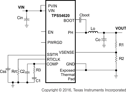
Simplified Schematic

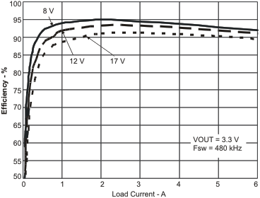
Efficiency vs Load Current

4 Revision History
Changes from E Revision (June 2016) to F Revision
- Updated data sheet text to our latest documentation and translations standardsGo
- Removed all references to the SwitcherPro™ Software Tool because it is no longer available for this partGo
- Moved storage temperature ratings to the Absolute Maximum Ratings tableGo
- Changed Handling Ratings table to ESD RatingsGo
- Changed RHY package to RHL in the Thermal Information tableGo
- Changed RGY values in the Thermal Information tableGo
- Updated packages in the last bullet point of Layout GuidelinesGo
- Added information to the last list item in Layout GuidelinesGo
Changes from D Revision (October 2014) to E Revision
- Added recommended layout guide lines for sensitive components and the output sensing trace to the Layout Guidelines section.Go
- Added Receiving Notification of Documentation Updates and Community Resources sections.Go
Changes from C Revision (April 2011) to D Revision
- Added the Device Information table, Handling Ratings table, the Recommended Operating Conditions table, and the Thermal Information tableGo
- Changed the Absolute Maximum Ratings for BOOT-PH, MAX value From: 7 V To: 7.7 V Go
- Changed Equation 28 From: C7(nF) To: C5(nF)Go
Changes from B Revision (October 2010) to C Revision
- Changed From separate RHL and RGY packages To a combined RHL and RGY packageGo
Changes from A Revision (January 2010) to B Revision
- Changed Small Signal Model for Frequency Compensation sectionGo
Changes from * Revision (May 2009) to A Revision
- Changed title from 17 V Input, 6 A Output, Synchronous Step Down Switcher with Integrated FET (SWIFT)Go
- Changed PowerPAD to Exposed Thermal PadGo
- Changed Changed the Absolute Maximum Ratings for EN, MAX value From: 3 V To: 6 VGo
- Changed minimum switching frequency min value from 180 to 160Go
- Changed minimum switching frequency max value from 220 to 240Go
- Added "Type 3" block around C11Go
- Changed PCB Layout graphicGo
5 Pin Configurations and Functions
Pin Functions
| PIN | I/O(1) | DESCRIPTION | |
|---|---|---|---|
| NAME | NO. | ||
| RT/CLK | 1 | I | Automatically selects between RT mode and CLK mode. An external timing resistor adjusts the switching frequency of the device; in CLK mode, the device synchronizes to an external clock. |
| GND | 2, 3 | G | Return for control circuitry and low-side power MOSFET. |
| PVIN | 4, 5 | P | Power input. Supplies the power switches of the power converter. |
| VIN | 6 | P | Supplies the control circuitry of the power converter. |
| VSENSE | 7 | I | Inverting input of the gm error amplifier. |
| COMP | 8 | O | Error amplifier output, and input to the output switch current comparator. Connect frequency compensation to this pin. |
| SS/TR | 9 | O | Slow-start and tracking. An external capacitor connected to this pin sets the internal voltage reference rise time. The voltage on this pin overrides the internal reference. It can be used for tracking and sequencing. |
| EN | 10 | I | Enable pin. Float to enable. Adjust the input undervoltage lockout with two resistors. |
| PH | 11, 12 | O | Switch node. |
| BOOT | 13 | I | A bootstrap cap is required between BOOT and PH. The voltage on this cap carries the gate drive voltage for the high-side MOSFET. |
| PWRGD | 14 | G | Power Good fault pin. Asserts low if output voltage is low because of thermal shutdown, dropout, over-voltage, EN shutdown, or during slow start. |
| Exposed Thermal PAD | 15 | G | Thermal pad of the package and signal ground and it must be soldered down for proper operation. |
