-
TPS6050x High-Efficiency, 250-mA Step-Down Charge Pump
- 1 Features
- 2 Applications
- 3 Description
- 4 Revision History
- 5 Device Comparison Table
- 6 Pin Configuration and Functions
- 7 Specifications
- 8 Detailed Description
- 9 Application and Implementation
- 10Power Supply Recommendations
- 11Layout
- 12Device and Documentation Support
- 13Mechanical, Packaging, and Orderable Information
- IMPORTANT NOTICE
Package Options
Mechanical Data (Package|Pins)
- DGS|10
Thermal pad, mechanical data (Package|Pins)
Orderable Information
TPS6050x High-Efficiency, 250-mA Step-Down Charge Pump
1 Features
- Wide Input Voltage Range From 1.8 V to 6.5 V
- Regulated 3.3-V, 1.8-V, 1.5-V, or Adjustable Output Voltage
- Up to 250-mA Output Current
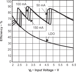
- Up to 90% Efficiency
- Output Voltage Tolerance 3% Over Line, Load, and Temperature Variation
- Device Quiescent Current Less Than 40 µA
- Output Voltage Supervisor Included (Power Good)
- Internal Soft Start
- Load Isolated From Battery During Shutdown
- Overtemperature and Overcurrent Protected
- Micro-Small 10-Pin VSSOP Package
- EVM Available, TPS60500EVM-193
2 Applications
- Mobile Phones
- Portable Instruments
- Internet Audio Player
- PC Peripherals
- USB Powered Applications
3 Description
The TPS6050x devices are a family of switched capacitor voltage converters, designed specifically for space-critical battery-powered applications.
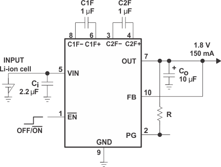
The TPS6050x step-down charge pumps generate a regulated, fixed 3.3-V, 1.8-V, 1.5-V, or adjustable output voltage. Only four small ceramic capacitors are required to build a complete high-efficiency DC–DC charge pump converter. To achieve the high efficiency over a wide input voltage range, the charge pump automatically selects between three different conversion modes. The output can deliver a maximum of 250-mA output current. The power good function supervises the output voltage and goes high when the output voltage rises to 97% of the nominal value.
The TPS6050x devices come in a micro-small 10-pin VSSOP package.
Device Information(1)
| PART NUMBER | PACKAGE | BODY SIZE (NOM) |
|---|---|---|
| TPS60500 TPS60501 TPS60502 TPS60503 |
VSSOP (10) | 3.05 mm × 4.98 mm |
- For all available packages, see the orderable addendum at the end of the data sheet.
Typical Application Schematic

Efficiency vs Input Voltage

4 Revision History
Changes from B Revision (February 2002) to C Revision
- Added Pin Configuration and Functions section, ESD Ratings table, Feature Description section, Device Functional Modes, Application and Implementation section, Power Supply Recommendations section, Layout section, Device and Documentation Support section, and Mechanical, Packaging, and Orderable Information section Go
5 Device Comparison Table
| PART NUMBER(1) | OUTPUT VOLTAGE [V] | MINIMUM INPUT VOLTAGE FOR IOUT = 150 mA |
|---|---|---|
| TPS60500DGS | Adjustable (0.8 V to 3.3 V) | VIN > VOUT + 1 |
| TPS60501DGS | 3.3 | VIN > 4.3 V |
| TPS60502DGS | 1.8 | VIN > 2.8 V |
| TPS60503DGS | 1.5 | VIN > 2.5 V |
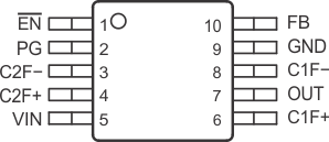
6 Pin Configuration and Functions

Pin Functions
| PIN | I/O | DESCRIPTION | |
|---|---|---|---|
| NAME | NO. | ||
| C1F+ | 6 | – | Positive terminal of the flying capacitor C1F |
| C1F− | 8 | – | Negative terminal of the flying capacitor C1F |
| C2F+ | 4 | – | Positive terminal of the flying capacitor C2F |
| C2F− | 3 | – | Negative terminal of the flying capacitor C2F |
| EN | 1 | I | Device-enable Input. − EN = High disables the device. Output and input are isolated in shutdown mode. − EN = Low enables the device. |
| GND | 9 | – | Ground |
| FB | 10 | O | TPS60500: connect via voltage divider to VO
TPS60501 to TPS60503: connect directly to VO |
| OUT | 7 | O | Regulated 3.3 V, 1.8 V, 1.5 V, or adjustable power output Bypass OUT to GND with the output filter capacitor Co. |
| PG | 2 | O | Open drain power good detector output. As soon as the voltage on OUT reaches about 97% of its nominal value this pin goes high. |
| VIN | 5 | I | Supply Input. Connect to an input supply in the 1.8-V to 6.5-V range. |