SLVS625E February 2006 – November 2015 TPS61150 , TPS61151
PRODUCTION DATA.
- 1 Features
- 2 Applications
- 3 Description
- 4 Revision History
- 5 Device Comparison Tables
- 6 Pin Configuration and Functions
- 7 Specifications
- 8 Detailed Description
- 9 Application and Implementation
- 10Power Supply Recommendations
- 11Layout
- 12Device and Documentation Support
- 13Mechanical, Packaging, and Orderable Information
Package Options
Mechanical Data (Package|Pins)
- DRC|10
Thermal pad, mechanical data (Package|Pins)
- DRC|10
Orderable Information
1 Features
2 Applications
- Sub- and Main-Display Backlight in Clamshell Phones
- Display and Keypad Backlight
- Up to 14-WLED Driver
3 Description
The TPS6115x is a high-frequency boost converter with two regulated current outputs for driving WLEDs. Each current output can be individually programmed through external resistors. There is a dedicated selection pin for each output so the two outputs can be turned on separately or simultaneously. The output current can be reduced by a pulse width modulation (PWM) signal on SEL pins or an analog voltage on the ISET pins, resulting in PWM dimming of the WLEDs. The boost regulator runs at a 1.2-MHz fixed switching frequency to reduce output ripple and avoid audible noises associated with pulse frequency modulation (PFM) control.
The two current outputs are ideal for driving WLED backlights for the sub and main displays in clamshell phones. The two outputs can also be used for driving display and keypad backlights. When used together, the two outputs can drive up to 14 WLEDs for one large display.
In addition to the small inductor, small capacitor, and 3-mm × 3-mm VSON package, the built-in MOSFET and diode eliminate the need for any external power devices. Overall, the device provides an extremely compact solution with high efficiency and plenty of flexibility.
Device Information(1)
| PART NUMBER | PACKAGE | BODY SIZE (NOM) |
|---|---|---|
| TPS61150 TPS61151 |
VSON (10) | 3.00 mm × 3.00 mm |
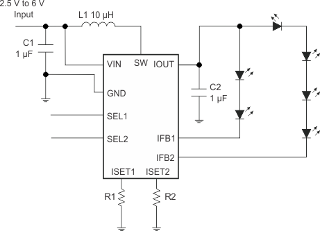
Typical Application
