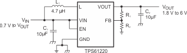
The TPS6122x family devices provide a power-supply solution for products powered by either a single-cell, two-cell, or three-cell alkaline, NiCd or NiMH, or one-cell Li-Ion or Li-polymer battery. Possible output currents depend on the input-to-output voltage ratio. The boost converter is based on a hysteretic controller topology using synchronous rectification to obtain maximum efficiency at minimal quiescent currents. The output voltage of the adjustable version can be programmed by an external resistor divider, or is set internally to a fixed output voltage. The converter can be switched off by a featured enable pin. While being switched off, battery drain is minimized. The device is offered in a 6-pin SC-70 package (DCK) measuring 2 mm x 2 mm to enable small circuit layout size.
PART NUMBER | PACKAGE | BODY SIZE (NOM) |
---|---|---|
TPS61220 | SC-70 (6) | 2.00mm x 1.25mm |
TPS61221 | ||
TPS61222 |
Changes from A Revision (April 2014) to B Revision
Changes from * Revision (August 2009) to A Revision
PIN | I/O | DESCRIPTION | |
---|---|---|---|
NAME | NO. | ||
EN | 6 | I | Enable input (1: enabled, 0: disabled). Must be actively tied high or low. Do not leave floating. |
FB | 2 | I | Voltage feedback of adjustable version. Must be connected to VOUT at fixed output voltage versions. |
GND | 3 | Control / logic and power ground | |
L | 5 | I | Connection for Inductor |
VIN | 1 | I | Boost converter input voltage |
VOUT | 4 | O | Boost converter output voltage |
TPS6122x | UNIT | ||
---|---|---|---|
VIN | Input voltage on VIN, L, VOUT, EN, FB | –0.3 to 7.5 | V |
TJ | Operating junction temperature | –40 to 150 | °C |
MIN | MAX | UNIT | |||
---|---|---|---|---|---|
Tstg | Storage temperature range | –65 | 150 | °C | |
V(ESD) | Electrostatic discharge | Human body model (HBM), per ANSI/ESDA/JEDEC JS-001, all pins(1) | –2 | 2 | kV |
Charged device model (CDM), per JEDEC specification JESD22-C101, all pins(2) | –1.5 | 1.5 | kV |
MIN | NOM | MAX | UNIT | ||
---|---|---|---|---|---|
VIN | Supply voltage at VIN | 0.7 | 5.5 | V | |
TJ | Operating virtual junction temperature | –40 | 125 | °C |
THERMAL METRIC(1) | TPS6122x | UNIT | |
---|---|---|---|
DCK | |||
6 PINS | |||
RθJA | Junction-to-ambient thermal resistance | 231.2 | °C/W |
RθJCtop | Junction-to-case (top) thermal resistance | 61.8 | |
RθJB | Junction-to-board thermal resistance | 78.8 | |
ψJT | Junction-to-top characterization parameter | 2.2 | |
ψJB | Junction-to-board characterization parameter | 78.0 | |
RθJCbot | Junction-to-case (bottom) thermal resistance | n/a |
PARAMETER | TEST CONDITIONS | MIN | TYP | MAX | UNIT | ||
---|---|---|---|---|---|---|---|
DC/DC STAGE | |||||||
VIN | Input voltage | 0.7 | 5.5 | V | |||
VIN | Minimum input voltage at startup | RLoad ≥ 150 Ω | 0.7 | V | |||
VOUT | TPS61220 output voltage | VIN < VOUT | 1.8 | 6.0 | V | ||
VFB | TPS61220 feedback voltage | 483 | 500 | 513 | mV | ||
VOUT | TPS61221 output voltage (3.3 V) | VIN < VOUT | 3.20 | 3.30 | 3.41 | V | |
VOUT | TPS61222 output voltage (5 V) | VIN < VOUT | 4.82 | 5.00 | 5.13 | V | |
ILH | Inductor current ripple | 200 | mA | ||||
ISW | switch current limit | VOUT = 3.3 V, VIN = 1.2 V, TA = 25°C | 240 | 400 | mA | ||
VOUT = 3.3 V | 200 | 400 | mA | ||||
RDSon_HSD | Rectifying switch on resistance | VOUT = 3.3 V | 1000 | mΩ | |||
VOUT = 5.0 V | 700 | mΩ | |||||
RDSon_LSD | Main switch on resistance | VOUT = 3.3 V | 600 | mΩ | |||
VOUT = 5.0 V | 550 | mΩ | |||||
Line regulation | VIN < VOUT | 0.5% | |||||
Load regulation | VIN < VOUT | 0.5% | |||||
IQ | Quiescent current | VIN | IO = 0 mA, VEN = VIN = 1.2 V, VOUT = 3.3 V |
0.5 | 0.9 | μA | |
VOUT | 5 | 7.5 | μA | ||||
ISD | Shutdown current | VIN | VEN = 0 V, VIN = 1.2 V, VOUT ≥ VIN | 0.2 | 0.5 | μA | |
ILKG_VOUT | Leakage current into VOUT | VEN = 0 V, VIN = 1.2 V, VOUT = 3.3 V | 1 | μA | |||
ILKG_L | Leakage current into L | VEN = 0 V, VIN = 1.2 V, VL = 1.2 V, VOUT ≥ VIN | 0.01 | 0.2 | μA | ||
IFB | TPS61220 Feedback input current | VFB = 0.5 V | 0.01 | μA | |||
IEN | EN input current | Clamped on GND or VIN (VIN < 1.5 V) | 0.005 | 0.1 | μA | ||
CONTROL STAGE | |||||||
VIL | EN input low voltage | VIN ≤ 1.5 V | 0.2 × VIN | V | |||
VIH | EN input high voltage | VIN ≤ 1.5 V | 0.8 × VIN | V | |||
VIL | EN input low voltage | 5 V > VIN > 1.5 V | 0.4 | V | |||
VIH | EN input high voltage | 5 V > VIN > 1.5 V | 1.2 | V | |||
VUVLO | Undervoltage lockout threshold for turn off | VIN decreasing | 0.5 | 0.7 | V | ||
Overvoltage protection threshold | 6.0 | 7.5 | V | ||||
Overtemperature protection | 140 | °C | |||||
Overtemperature hysteresis | 20 | °C |
TABLE OF GRAPHS | FIGURE | |
---|---|---|
Maximum Output Current | versus Input Voltage (TPS61220, TPS61221, TPS61222) | Figure 1 |
Efficiency | versus Output Current, VOUT = 1.8 V, VIN = [0.7 V; 1.2 V; 1.5 V] (TPS61220) | Figure 2 |
versus Output Current, VIN = [0.7 V; 1.2 V; 2.4 V; 3 V] (TPS61221) | Figure 3 | |
versus Output Current, VIN = [0.7 V; 1.2 V; 2.4V; 3.6 V; 4.2 V] (TPS61222) | Figure 4 | |
versus Input Voltage, VOUT = 1.8 V, IOUT = [100 µA; 1 mA; 10 mA; 50 mA] (TPS61220) | Figure 5 | |
versus Input Voltage, IOUT = [100 µA; 1 mA; 10 mA; 50 mA] (TPS61221) | Figure 6 | |
versus Input Voltage, IOUT = [100 µA; 1 mA; 10 mA; 50 mA] (TPS61222) | Figure 7 | |
Input Current | at No Output Load, Device Enabled (TPS61220, TPS61221, TPS61222) | Figure 8 |
Output Voltage | versus Output Current, VOUT = 1.8 V, VIN = [0.7 V; 1.2 V] (TPS61220 ) | Figure 9 |
versus Output Current, VIN = [0.7 V; 1.2 V; 2.4 V] (TPS61221) | Figure 10 | |
versus Output Current, VIN = [0.7 V; 1.2 V; 2.4 V; 3.6 V] (TPS61222) | Figure 11 | |
versus Input Voltage, Device Disabled, RLOAD = [1 kΩ; 10 kΩ] (TPS6122x) | Figure 12 | |
Waveforms | Output Voltage Ripple, VIN = 0.8 V, VOUT = 1.8 V, IOUT = 20 mA (TPS61220) | Figure 13 |
Output Voltage Ripple VIN = 1.8 V, IOUT = 50 mA (TPS61221) | Figure 14 | |
Load Transient Response, VIN = 1.2 V, IOUT = 6 mA to 50 mA (TPS61221) | Figure 15 | |
Load Transient Response, VIN = 2.4 V, IOUT = 14 mA to 126 mA (TPS61222) | Figure 16 | |
Line Transient Response, VIN = 1.8 V to 2.4 V, RLOAD = 100 Ω (TPS61221) | Figure 17 | |
Line Transient Response, VIN = 2.8 V to 3.6 V, RLOAD = 100 Ω (TPS61222) | Figure 18 | |
Startup after Enable, VIN = 0.7 V, VOUT = 1.8 V, RLOAD = 150 Ω (TPS61220) | Figure 19 | |
Startup after Enable, VIN = 0.7 V, RLOAD = 150 Ω, (TPS61222) | Figure 20 | |
Continuous Current Operation, VIN = 1.2 V, VOUT = 1.8 V, IOUT = 50mA (TPS61220 ) | Figure 21 | |
Discontinuous Current Operation, VIN = 1.2 V, VOUT = 1.8 V, IOUT = 10mA (TPS61220) | Figure 22 |
VO = 3.3 V | ||
VO = 1.8 V | ||
VO = 5 V | ||
VO = 1.8 V | ||
VO = 5 V | ||
VI = 0.8 V | VO = 1.8 V | IO = 20 mA |
VI = 1.2 V | IO = 6 mA to 50 mA | |
VI = 2.4 V to 2.4 V | RLOAD = 100 Ω | trise = tfall = 20 ms |
VI = 0.7 V | VO = 1.8 V | RLOAD = 150 Ω |
VI = 1.2 V | VO = 1.8 V | IO = 50 mA |
VO = 1.8 V | ||
VO = 5 V | ||
VO = 3.3 V | ||
Device enabled | ||
VO = 3.3 V | ||
VEN = 0 V | ||
VI = 1.8 V | VO = 3.3 V | IO = 50 mA |
VI = 2.4 V | IO = 14 mA to 126 mA | |
VI = 2.8 V to 3.6 V | RLOAD = 100 Ω | trise = tfall = 20 ms |
VI = 0.7 V | VO = 3.3 V | RLOAD = 50 Ω |
VI = 1.2 V | VO = 1.8 V | IO = 10 mA |
COMPONENT REFERENCE | PART NUMBER | MANUFACTURER | VALUE | |
---|---|---|---|---|
C1 | GRM188R60J106ME84D | Murata | 10 μF, 6.3V. X5R Ceramic | |
C2 | GRM188R60J106ME84D | Murata | 10 μF, 6.3V. X5R Ceramic | |
L1 | EPL3015-472MLB | Coilcraft | 4.7 μH | |
R1, R2 | adjustable version: Values depending on the programmed output voltage | |||
fixed version: R1= 0 Ω, R2 not used |