-
TPS62134x, 17-V Input, Step-down Converter With Low-Power Mode Input for Intel Skylake Platform
- 1 Features
- 2 Applications
- 3 Description
- 4 Revision History
- 5 Device Comparison Table
- 6 Pin Configuration and Functions
- 7 Specifications
-
8 Detailed Description
- 8.1 Overview
- 8.2 Functional Block Diagram
- 8.3
Feature Description
- 8.3.1 Enable and Shutdown (EN)
- 8.3.2 Undervoltage Lockout (UVLO)
- 8.3.3 Soft-Start (SS) Circuitry
- 8.3.4 Switch Current-Limit and Short Circuit Protection
- 8.3.5 Output Voltage and LPM Logic Selection (VIDx and LPM)
- 8.3.6 Power-Good Output (PG)
- 8.3.7 Single-Ended Remote Sense (FBS)
- 8.3.8 Thermal Shutdown
- 8.4 Device Functional Modes
- 9 Application and Implementation
- 10Power Supply Recommendations
- 11Layout
- 12Device and Documentation Support
- 13Mechanical, Packaging, and Orderable Information
- IMPORTANT NOTICE
Package Options
Mechanical Data (Package|Pins)
- RGT|16
Thermal pad, mechanical data (Package|Pins)
- RGT|16
Orderable Information
TPS62134x, 17-V Input, Step-down Converter With Low-Power Mode Input for Intel Skylake Platform
1 Features
- DCS-Control™ Architecture
- Supports Low-Power Mode for System Standby Mode
- Power Save Mode for Light Load Efficiency
- Selectable Fixed Output Voltage (0.7 V to 1.05 V)
- Low Power Mode Logic Input
- Quiescent Current of 20 µA
- Input Voltage Range: 3 V to 17 V
- Output Current: up to 3.2 A
- Programmable Soft Start
- Power Good Output
- Short Circuit Protection
- Single-ended Remote Sense
- Thermal Shutdown Protection
- Available in a 3-mm × 3-mm, VQFN-16 Package
2 Applications
- Intel Skylake™ Platform Ultrabook, Notebook, PC
- Standard 12-V Rail Supply
- POL Supply from 1 to 4 Cells Li-Ion Battery
- Solid-State Disk Drive
- Embedded System
3 Description
The TPS62134x family of devices is an easy-to-use, synchronous step-down DC-DC converter, compatible with Intel Skylake platform applications such as Ultrabooks™ and notebooks. The high performance DCS-Control™ architecture provides fast transient response as well as high output voltage accuracy.
With a wide operating input-voltage range of 3 to 17 V, the devices are ideally suited for systems powered from either a Li-Ion or other batteries as well as from 12-V intermediate power rails. The devices have a low-power mode where the output voltage is reduced by using the LPM pin. In addition, the devices support dynamic output-voltage change by using the VIDx pins. The LPM and VIDx pins help the system minimize power consumption in different operating modes.
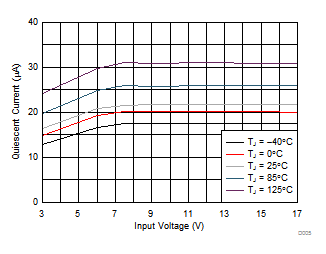
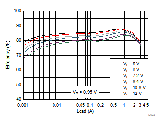
The output-voltage startup ramp is controlled by the SS pin. The power sequencing is configurable by the enable (EN) and power good (PG) pins. In power-save mode, the devices show quiescent current of approximately 20 μA which maintains high efficiency over the entire load range. Short circuit protection and thermal shutdown protect the IC and external components from heavy current when the output is shorted to ground. The device is available in a 3-mm × 3-mm 16-pin VQFN package with thermal pad.
Device Information(1)
| PART NUMBER | PACKAGE | BODY SIZE (NOM) |
|---|---|---|
| TPS62134A | VQFN | 3.00mm x 3.00mm |
| TPS62134B | ||
| TPS62134C | ||
| TPS62134D |
- For all available packages, see the orderable addendum at the end of the data sheet.
spacer
spacer
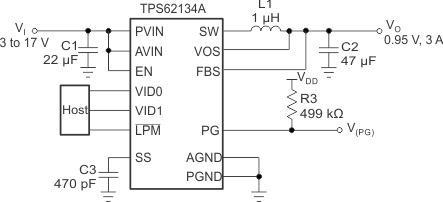
Typical Application Circuit
TPS62134A Efficiency
4 Revision History
Changes from D Revision (April 2015) to E Revision
- Added Note to Power-Good Output (PG). PG blanking time condition for TPS62134A and TPS62134C Go
Changes from C Revision (January 2015) to D Revision
- Added the Program Output Voltage with External Resistor Divider sectionGo
Changes from B Revision (August 2014) to C Revision
- Changed the Device Information table Go
- Added the Device Comparison Table Go
- Moved the Storage temperature From the Handling Ratings table to the Absolute Maximum Ratings tableGo
- Changed the Handling Ratings table to the ESD Ratings tableGo
- Changed the Output voltage accuracy, PSM mode MAX value From: 2% To: 3%, Add test condition: LPM = High.Go
Changes from A Revision (August 2014) to B Revision
- Add new device to Device Comparison TableGo
- Updated the Functional Block Diagram imageGo
- Add new device to Table 1Go
- Updated the Figure 16 in the Application Curves sectionGo
- Updated Equation 8 Go
Changes from * Revision (August 2014) to A Revision
- Switched the pin names of pin 8 and 9 in the Pin Functions tableGo
5 Device Comparison Table
| PART NUMBER | PACKAGE MARKING | OUTPUT VOLTAGE |
|---|---|---|
| TPS62134A | 134A | See Table 1 |
| TPS62134B | 134B | |
| TPS62134C | 134C | |
| TPS62134D | 134D |
6 Pin Configuration and Functions
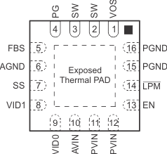
Pin Functions
7 Specifications
7.1 Absolute Maximum Ratings(1)
over operating junction temperature range (unless otherwise noted)| MIN | MAX | UNIT | ||
|---|---|---|---|---|
| Voltage at pins(2) | AVIN, PVIN | –0.3 | 20 | V |
| EN, SW | –0.3 | VI + 0.3 | ||
| SS, PG, VOS, VID0, VID1, LPM | –0.3 | 7 | ||
| FBS | –0.3 | 3 | ||
| Sink current | PG | 0 | 2 | mA |
| Operating junction temperature, TJ | –40 | 150 | °C | |
| Storage temperature, Tstg | –65 | 150 | °C | |
7.2 ESD Ratings
| VALUE | UNIT | |||
|---|---|---|---|---|
| V(ESD) | Electrostatic discharge | Human body model (HBM), per ANSI/ESDA/JEDEC JS–001 (1) | ±2000 | V |
| Charged device model (CDM), per JEDEC specification JESD22-C101(2) | ±500 | |||
7.3 Recommend Operating Conditions
over operating junction temperature range, unless otherwise noted.| MIN | MAX | UNIT | |||
|---|---|---|---|---|---|
| VI | Input voltage (AVIN, PVIN) | 3 | 17 | V | |
| V(PG) | PG pin pullup resistor voltage | 0 | 6 | V | |
| IO | Output current | 3 V ≤ VI < 5 V | 0 | 3 | A |
| 5 V ≤ VI ≤ 17 V | 0 | 3.2 | |||
| TJ | Operating junction temperature | –40 | 125 | °C | |
7.4 Thermal Information
| THERMAL METRIC(1) | TPS62134x | UNIT | |
|---|---|---|---|
| RGT (VQFN) | |||
| 16 PINS | |||
| RθJA | Junction-to-ambient thermal resistance | 44.2 | °C/W |
| RθJC(top) | Junction-to-case (top) thermal resistance | 51.0 | |
| RθJB | Junction-to-board thermal resistance | 16.6 | |
| ψJT | Junction-to-top characterization parameter | 0.9 | |
| ψJB | Junction-to-board characterization parameter | 16.6 | |
| RθJC(bot) | Junction-to-case (bottom) thermal resistance | 3.7 | |
Electrical Characteristic
TJ = –40 °C to 125 °C and VI = 3 V to 17 V. Typical values at VI = 12 V and TJ = 25 °C, unless otherwise noted.| PARAMETER | TEST CONDITIONS | MIN | TYP | MAX | UNIT | ||
|---|---|---|---|---|---|---|---|
| SUPPLY | |||||||
| VI | Input voltage range | 3 | 17 | V | |||
| IQ | Operating quiescent current | EN = High, no load, device not switching TJ = –40 °C to 85 °C |
20 | 35 | µA | ||
| TJ = 125 °C | 58 | ||||||
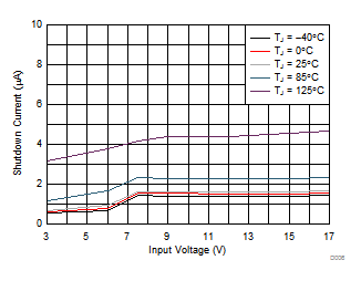
| ISD | Shutdown current into AVIN and PVIN | EN = Low TJ = –40 °C to +85 °C |
2 | 9 | µA | ||
| TJ = 125 °C | 18 | ||||||
| V(UVLO) | Undervoltage lockout threshold | VI falling | 2.6 | 2.7 | 2.8 | V | |
| VI rising | 2.8 | 2.9 | 3 | ||||
| TSD(th) | Thermal shutdown threshold | TJ rising | 160 | °C | |||
| TSD(hys) | Thermal shutdown hysteresis | TJ falling | 20 | ||||
| CONTROL (EN, SS, PG, VIDx, LPM) | |||||||
| VIH | High-level input threshold voltage (EN, VIDx, LPM) | 0.8 | 0.54 | V | |||
| VIL | Low-level input threshold voltage (EN, VIDx, LPM) | 0.47 | 0.3 | V | |||
| R(PD) | Pull down resistor at EN, VIDx, LPM | EN, VIDx, LPM = low | 400 | kΩ | |||
| R(DIS) | Output discharge resistor | EN = Low, VO = 1 V | 20 | kΩ | |||
| Ilkg | Input leakage current at EN, VIDx, LPM | EN, VIDx, LPM = 3.3 V | 0.01 | 1 | µA | ||
| VTH(PG) | Power good threshold DC voltage | VO rising | 736 | 760 | 784 | mV | |
| VO falling | 696 | 720 | 752 | ||||
| VOL(PG) | Power good output low voltage | I(PG) = –2 mA | 0.07 | 0.3 | V | ||
| Ilkg(PG) | Input leakage current at PG | V(PG) = 1.8 V | 1 | 400 | nA | ||
| td(PG) | Power good delay time | PG rising | 140 | µs | |||
| PG falling | 20 | ||||||
| I(SS) | SS pin source current | 2.3 | 2.5 | 2.7 | µA | ||
| POWER SWITCH | |||||||
| rDS(on_H) | High-side MOSFET on-resistance | VI ≥ 6 V | 90 | 170 | mΩ | ||
| rDS(on_L) | Low-side MOSFET on-resistance | VI ≥ 6 V | 40 | 70 | |||
| IL | High-side MOSFET DC current-limit | VI ≥ 5 V, TJ = 25 °C | 3.6 | 4.4 | 5.4 | A | |
| IL(LOW) | High-side MOSFET DC current-limit at low output voltage | VO ≤ 0.3 V | 1.6 | ||||
| OUTPUT | |||||||
| Ilkg(FBS) | Input leakage current at FBS | V(FBS)= 1.1 V | 1 | 100 | nA | ||
| VO(A) | Output voltage accuracy | PWM mode | –1% | 1% | |||
| PSM mode, LPM = High(1) | –1% | 3% | |||||
| ΔVO(ΔIO) | Load regulation(2) | VI = 7.2 V, IO = 0.5 A to 3.2 A | 0.01 | %/A | |||
| ΔVO(ΔVI) | Line regulation(2) | 3 V ≤ VI ≤ 17 V, IO = 1 A | 0.003 | %/V | |||
7.5 Typical Characteristics
