-
TPS6216x 3-V to 17-V, 1-A Step-Down Converters with DCS-Control™
- 1 Features
- 2 Applications
- 3 Description
- 4 Revision History
- 5 Device Voltage Options
- 6 Pin Configuration and Functions
- 7 Specifications
- 8 Detailed Description
- 9 Application and Implementation
- 10Power Supply Recommendations
- 11Layout
- 12Device and Documentation Support
- 13Mechanical, Packaging, and Orderable Information
- IMPORTANT NOTICE
Package Options
Mechanical Data (Package|Pins)
- DSG|8
Thermal pad, mechanical data (Package|Pins)
- DSG|8
Orderable Information
TPS6216x 3-V to 17-V, 1-A Step-Down Converters with DCS-Control™
1 Features
- DCS-Control™ Topology
- Input Voltage Range from 3 V to 17 V
- Up to 1-A Output Current
- Adjustable Output Voltage From 0.9 V to 6 V
- Fixed Output Voltage Versions
- Seamless Power Save Mode Transition
- Typically 17-µA Quiescent Current
- Power Good Output
- 100% Duty Cycle Mode
- Short Circuit Protection
- Over Temperature Protection
- Pin to Pin Compatible With TPS62170 and TPS62125
- Available in 3.00 mm x 3.00 mm 8-Pin VSSOP and 2.00 mm × 2.00 mm 8-Pin WSON Packages
- Create a Custom Design using the TPS62160 with the WEBENCH® Power Designer
2 Applications
- Standard 12-V Rail Supplies
- POL Supply From Single or Multiple Li-Ion Battery
- LDO Replacement
- Embedded Systems
- Digital Still Camera, Video
- Mobile PCs, Tablet-PCs, Modems
3 Description
The TPS6216x device family are easy to use synchronous step-down DC/DC converters optimized for applications with high power density. A high switching frequency of typically 2.25 MHz allows the use of small inductors and provides fast transient response as well as high output voltage accuracy by utilization of the DCS-Control™ topology.
With its wide operating input voltage range of 3 V to 17 V, the devices are ideally suited for systems powered from either a Li-Ion or other battery as well as from 12-V intermediate power rails. It supports up to 1-A continuous output current at output voltages between 0.9 V and 6 V (with 100% duty cycle mode).
Power sequencing is also possible by configuring the enable and open-drain power good pins.
In power save mode, the devices show quiescent current of about 17 μA from VIN. Power save mode, entered automatically and seamlessly if the load is small, maintains high efficiency over the entire load range. In shutdown mode, the device is turned off and shutdown current consumption is less than 2 μA.
The device, available in adjustable and fixed output voltage versions, is packaged in an 8-pin WSON package measuring 2.00 mm × 2.00 mm (DSG) or 8-pin VSSOP package measuring 3.00 mm x 3.00 mm (DGK).
Device Information(1)
| PART NUMBER | PACKAGE | BODY SIZE (NOM) |
|---|---|---|
| TPS6216x | WSON (8) | 2.00 mm x 2.00 mm |
| TPS62160 | VSSOP (8) | 3.00 mm x 3.00 mm |
- For all available packages, see the orderable addendum at the end of the datasheet.
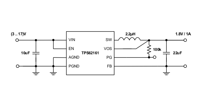
Typical Application Schematic

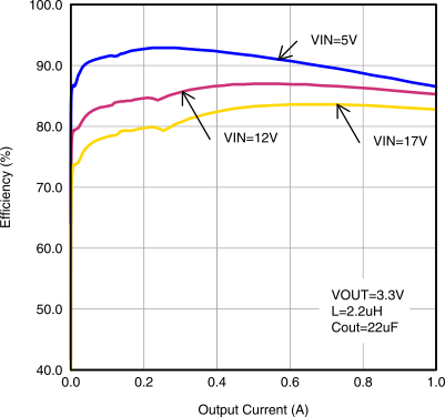
Efficiency vs Output Current

4 Revision History
Changes from D Revision (October 2014) to E Revision
- Added link to WEBENCH® Designer Go
- Added "SW (AC), less than 10ns" specification to Absolute Maximum Ratings tableGo
- Changed TJ MAX spec from "125" to "150" Go
- Added IQ and ISD specificationsGo
- Added 125°C plot line in Figure 1 and Figure 4 Typical Characteristics graphic entities. Go
Changes from C Revision (September 2013) to D Revision
- Added Device Information and ESD Ratings tables, Feature Description section, Device Functional Modes, Application and Implementation section, Power Supply Recommendations section, Layout section, Device and Documentation Support section, and Mechanical, Packaging, and Orderable Information section.Go
Changes from B Revision (August 2013) to C Revision
- Changed 50mV/μs to 50mV/s in Enable / Shutdown (EN) section Go
Changes from A Revision (March 2012) to B Revision
- Added note to Terminal FunctionsGo
- Changed Equation 13Go
- Added diode to Figure 41Go
Changes from * Revision (November 2011) to A Revision
5 Device Voltage Options
| OUTPUT VOLTAGE(1) | PART NUMBER | PACKAGE |
|---|---|---|
| adjustable | TPS62160 | WSON (8) |
| 1.8 V | TPS62161 | |
| 3.3 V | TPS62162 | |
| 5.0 V | TPS62163 | |
| adjustable | TPS62160 | VSSOP (8) |
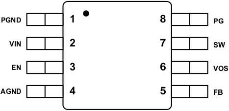
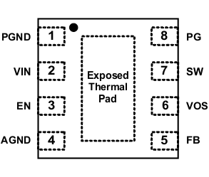
6 Pin Configuration and Functions

Pin Functions
| PIN(1) | I/O | DESCRIPTION | |
|---|---|---|---|
| NAME | NO. | ||
| PGND | 1 | — | Power ground |
| VIN | 2 | I | Supply voltage |
| EN | 3 | I | Enable input (High = enabled, Low = disabled) |
| AGND | 4 | — | Analog ground |
| FB | 5 | I | Voltage feedback of adjustable version. Connect resistive voltage divider to this pin. It is recommended to connect FB to AGND on fixed output voltage versions for improved thermal performance. |
| VOS | 6 | I | Output voltage sense pin and connection for the control loop circuitry. |
| SW | 7 | O | Switch node, which is connected to the internal MOSFET switches. Connect inductor between SW and output capacitor. |
| PG | 8 | O | Output power good (High = VOUT ready, Low = VOUT below nominal regulation); open drain (requires pull-up resistor; goes high impedance, when device is switched off) |
| Exposed Thermal Pad(2) | — | Must be connected to AGND. Must be soldered to achieve appropriate power dissipation and mechanical reliability. | |
