-
TPS6218x 4-V to 15-V, 6-A, 2-Phase Step-Down Converters with AEE
- 1 Features
- 2 Applications
- 3 Description
- 4 Revision History
- 5 Device Comparison Table
- 6 Pin Configuration and Functions
- 7 Specifications
-
8 Detailed Description
- 8.1 Overview
- 8.2 Functional Block Diagram
- 8.3 Feature Description
- 8.4
Device Functional Modes
- 8.4.1 Pulse Width Modulation (PWM) Operation
- 8.4.2 Power Save Mode (PSM) Operation
- 8.4.3 Minimum Duty Cycle and 100% Mode Operation
- 8.4.4 Automatic Efficiency Enhancement (AEE)
- 8.4.5 Phase-Shifted Operation
- 8.4.6 Current Limit, Current Balancing, and Short Circuit Protection
- 8.4.7 Tracking
- 8.4.8 Operation with Fixed VOUT
- 9 Application and Implementation
- 10Power Supply Recommendations
- 11Layout
- 12Device and Documentation Support
- 13Mechanical, Packaging, and Orderable Information
- IMPORTANT NOTICE
Package Options
Mechanical Data (Package|Pins)
- YZF|24
Thermal pad, mechanical data (Package|Pins)
Orderable Information
TPS6218x 4-V to 15-V, 6-A, 2-Phase Step-Down Converters with AEE
1 Features
- Dual Phase Balanced Peak Current Mode
- Input Voltage Range: 4 V to 15 V
- Output Voltage Range: 0.9 V to 6 V
- Output Current up to 6 A
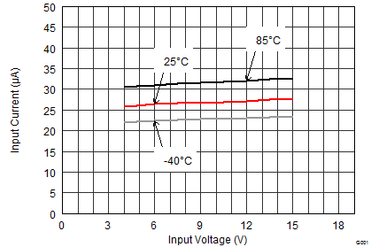
- Typical Quiescent Current of 28 µA
- Output Voltage Accuracy of ±1% (PWM Mode)
- Automatic Efficiency Enhancement (AEE™)
- Phase Shifted Operation
- Automatic Power Save Mode
- Adjustable Soft Start
- Power Good Output
- Undervoltage Lockout
- HICCUP Over Current Protection
- Pin-to-Pin Compatible with TPS62184
- Over Temperature Protection
- NanoFree™ 2.10 mm x 3.10 mm DSBGA Package
- Create a Custom Design Using the TPS62180 With the WEBENCH® Power Designer
2 Applications
- Low Profile POL Supply
- NVDC Powered Systems
- Dual/Triple Cell Li-ion Battery
- Ultra Portable/Embedded/Tablet PC
- Computing Network Solutions
- Micro Server, SSD
3 Description
The TPS6218x is a synchronous dual-phase step-down DC-DC converter for low profile power rails. It operates with two identical, current balanced phases that are peak current controlled enabling use in height limited applications.
With a wide operating input voltage range of 4 V to 15 V, the device is ideally suited for systems powered from multi-cell Li-Ion batteries or 12-V rails. The output current of 6 A is continuously provided by two phases of 3 A each, allowing the use of low profile external components. The phases operate out of phase, reducing switching noise significantly.
The TPS6218x automatically enters Power Save Mode to maintain high efficiency down to very light loads. It also incorporates an Automatic Efficiency Enhancement (AEE™) for the entire duty cycle range.
The device features a Power Good signal, as well as an adjustable soft start. The quiescent current is typically 28 µA, it is able to run in 100% mode, and it has no duty cycle limitation even at lowest output voltage.
The TPS6218x, available in adjustable and fixed output voltage options, is packaged in a small 24-bump, 0.5 mm pitch DSBGA package.
Device Information(1)
| PART NUMBER | PACKAGE | BODY SIZE (NOM) |
|---|---|---|
| TPS62180 | DSBGA (24) | 2.10 mm x 3.10 mm |
| TPS62182 | DSBGA (24) | 2.10 mm x 3.10 mm |
- For all available packages, see the orderable addendum at the end of the datasheet.
spacing
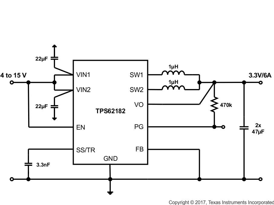
Simplified Schematic
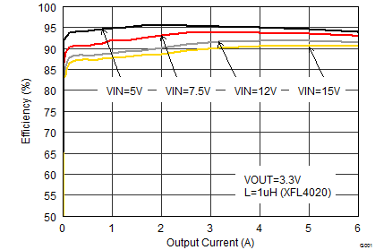
Efficiency vs Output Current
4 Revision History
Changes from A Revision (August 2014) to B Revision
- Added Feature: Pin-to-Pin Compatible with TPS62184Go
- Added WEBENCH® information to Features, Detailed Design Procedures, and Development Support sections.Go
- Changed the BODY SIZE value From: 2.14 mm x 3.14 mm To: 2.10 mm x 3.10 mm in the Device Information tableGo
- Added SW1, SW2, (AC, less than 10ns) and Note (3) to the Pin voltage range in the Absolute Maximum Ratings tableGo
- Changed Handling Ratings To: ESD Ratings tableGo
- Added Table 1 Go
- Added the application note Go
- Changed the Design Requirements paragraphGo
- Added Note (2) to Table 6 Go
- Added Figure 31 and Figure 32Go
- Added Figure 37 Go
- Changed the Design Requirements paragraphGo
- Added Figure 38 and Figure 39 to the Inductor sectionGo
- Changed Figure 55 Go
Changes from * Revision (August 2014) to A Revision
- Released to Production Go
5 Device Comparison Table
| PART NUMBER | OUTPUT VOLTAGE | TJ |
|---|---|---|
| TPS62180 | Adjustable | -40°C to 125°C |
| TPS62182 | 3.3 V | -40°C to 125°C |
Spacer
6 Pin Configuration and Functions

Pin Functions
| PIN(1) | DESCRIPTION | |
|---|---|---|
| NAME | NUMBER | |
| AGND | C4 | Analog Ground. Connect on PCB directly with PGND. |
| EN | E4 | Enable input (High = enabled, Low = disabled) |
| FB | B4 | Output voltage feedback. Connect resistive voltage divider to this pin and AGND. On TPS62182, connect to AGND. |
| PG | F4 | Output power good (High = VOUT ready, Low = VOUT below nominal regulation); open drain (requires pull-up resistor) |
| PGND | A3, B3, C3, D3, E3, F3 | Common power ground. |
| SS/TR | D4 | Soft-Start and Tracking Pin. An external capacitor connected to this pin sets the internal voltage reference rise time. |
| SW1 | A2, B2, C2 | Switch node for Phase 1 (master), connected to the internal MOSFET switches. Connect inductor 1 between SW1 and output capacitor. |
| SW2 | D2, E2, F2 | Switch node for Phase 2 (follower), connected to the internal MOSFET switches. Connect inductor 2 between SW2 and output capacitor. |
| VIN1 | A1, B1, C1 | Supply voltage for Phase 1. |
| VIN2 | D1, E1, F1 | Supply voltage for Phase 2. |
| VO | A4 | Output Voltage Connection |
7 Specifications
7.1 Absolute Maximum Ratings(1)
| MIN | MAX | UNIT | ||
|---|---|---|---|---|
| Pin voltage range(2) | VIN1, VIN2 | –0.3 | 17 | V |
| EN, PG | –0.3 | VIN + 0.3 | V | |
| SW1, SW2, (DC) | –0.3 | VIN + 0.3 | V | |
| SW1, SW2, (AC, less than 10ns)(3) | –2 | 24.5 | ||
| SS/TR | –0.3 | VIN + 0.3, but ≤ 7 |
V | |
| FB, VO | –0.3 | 7 | V | |
| Power good sink current | PG | 10 | mA | |
| Operating junction temperature range | TJ | –40 | 150 | °C |
| Storage Temperature Range | Tstg | –65 | 150 | °C |
7.2 ESD Ratings
| MIN | MAX | UNIT | ||
|---|---|---|---|---|
| VESD(1) | Human Body Model (HBM) ESD stress voltage(2) | –1 | 1 | kV |
| Charge device model (CDM) ESD stress voltage | –0.5 | 0.5 | ||
7.3 Recommended Operating Conditions
| MIN | TYP | MAX | UNIT | ||
|---|---|---|---|---|---|
| Supply voltage range, VIN | 4 | 15 | V | ||
| Output voltage range, VOUT | 0.9 | 6 | V | ||
| Maximum Output current, IOUT(max) | 0.9V ≤ VOUT ≤ 3.3V | 6 | A | ||
| 3.3V < VOUT | 6 | ||||
| Operating junction temperature, TJ | –40 | 125 | °C | ||
7.4 Thermal Information
| THERMAL METRIC(1) | TPS6218x | UNIT | |
|---|---|---|---|
| YZF (24 PINS) | |||
| RθJA | Junction-to-ambient thermal resistance | 61.5 | °C/W |
| RθJCtop | Junction-to-case (top) thermal resistance | 0.3 | °C/W |
| RθJB | Junction-to-board thermal resistance | 10.1 | °C/W |
| ψJT | Junction-to-top characterization parameter | 0.1 | °C/W |
| ψJB | Junction-to-board characterization parameter | 10.1 | °C/W |
| RθJCbot | Junction-to-case (bottom) thermal resistance | n/a | °C/W |
7.5 Electrical Characteristics
Over operating junction temperature range (TJ = –40°C to +125°C) and VIN = 4 V to 15 V.Typical values at VIN = 12 V and TJ = 25°C (unless otherwise noted).
| PARAMETER | TEST CONDITIONS | MIN | TYP | MAX | UNIT | ||
|---|---|---|---|---|---|---|---|
| SUPPLY | |||||||
| VIN | Input voltage range | 4 | 15 | V | |||
| IQ | Operating quiescent current | EN = High, IOUT = 0 mA, Device not switching, (TJ = –40°C to +85°C) |
28 | 55 | µA | ||
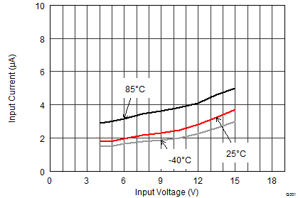
| ISD | Shutdown current | EN = Low (≤ 0.3 V), (TJ = –40°C to +85°C) | 2.8 | 15 | µA | ||
| VUVLO | Undervoltage lockout threshold (1) | Falling input voltage | 3.5 | 3.6 | 3.7 | V | |
| Hysteresis | 300 | mV | |||||
| TSD | Thermal shutdown | Rising junction temperature | 160 | °C | |||
| Hysteresis | 20 | ||||||
| CONTROL (EN, SS/TR, PG) | |||||||
| VH_EN | High-level input threshold voltage (EN) | 0.97 | 1 | 1.03 | V | ||
| VL_EN | Low-level input threshold voltage (EN) | 0.87 | 0.9 | 0.93 | V | ||
| ILKG_EN | Input leakage current (EN) | EN = VIN or GND | 0.01 | 1.2 | µA | ||
| ISS/TR | SS/TR pin source current | 4.5 | 5 | 5.5 | µA | ||
| VTH_PG | Power good threshold voltage | Rising (%VOUT) | 94% | 96% | 98% | ||
| Falling (%VOUT) | 90% | 92% | 94% | ||||
| VOL_PG | Power good output low voltage | IPG= -2 mA | 0.3 | V | |||
| ILKG_PG | Input leakage current (PG) | 1 | 100 | nA | |||
| POWER SWITCH | |||||||
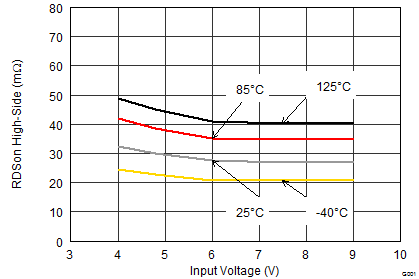
| RDS(ON) | High-side MOSFET ON-resistance | VIN = 7.5 V | Phase 1 | 27 | 65 | mΩ | |
| Phase 2 | |||||||
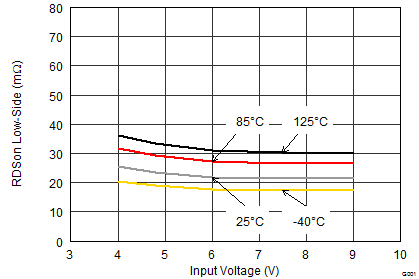
| Low-side MOSFET ON-resistance | Phase 1 | 21 | 45 | mΩ | |||
| Phase 2 | |||||||
| ILIM | High-side MOSFET current limit | Each phase, VIN = 7.5 V | 4.0 | 4.7 | 5.5 | A | |
| TPSD | Phase shift delay time | Phase 2 after Phase 1, PWM mode | 250 | ns | |||
| OUTPUT | |||||||
| VREF | Internal reference voltage | 0.792 | 0.8 | 0.808 | V | ||
| ILKG_FB | Input leakage current (FB) | VFB = 0.8 V | 1 | 100 | nA | ||
| RDISCHARGE | Output discharge resistance | EN = Low | 60 | Ω | |||
| VOUT | Output voltage range (TPS62180) | VIN ≥ VOUT | 0.9 | 6 | V | ||
| Output voltage (TPS62182) | 3.3 | V | |||||
| Feedback voltage accuracy (TPS62180)(2) |
PWM Mode, VIN ≥ VOUT + 1 V | –1% | 1% | ||||
| Power Save Mode, VOUT = 3.3 V, Iload ≥ 1 mA, L = 1 µH, COUT = 2 x 47 µF, (TJ = –40°C to +85°C) |
–1% | 2% | |||||
| Power Save Mode, VOUT = 1.8 V, Iload ≥ 1 mA, L = 1 µH, COUT = 4 x 47 µF, (TJ = –40°C to +85°C) |
|||||||
| Power Save Mode, VOUT = 0.9 V, Iload ≥ 1 mA, L = 1 µH, COUT = 4 x 47 µF, (TJ = –40°C to +85°C) |
–1% | 3% | |||||
| Output voltage accuracy (TPS62182)(2) |
PWM Mode, VIN ≥ VOUT + 1 V | –1% | 1% | ||||
| Power Save Mode, Iload ≥ 1 mA, L = 1 µH, COUT = 2 x 47 µF, (TJ = –40°C to +85°C) |
–1% | 2% | |||||
| Load regulation | VOUT = 3.3 V, PWM Mode operation | 0.04 | %/A | ||||
| Line regulation | 4 V ≤ VIN ≤ 15 V, VOUT = 3.3 V, IOUT = 4 A | 0.01 | %/V | ||||
| tHICCUP | Hiccup on time | 0.9 | ms | ||||
| Hiccup off time | 5 | ||||||
7.6 Typical Characteristics
