-
TPS6256x 2.25-MHz, 600-mA Step-Down Converter in TSOT and 2 × 2 × 0.8-mm QFN Package
- 1 Features
- 2 Applications
- 3 Description
- 4 Revision History
- 5 Device Comparison Table
- 6 Pin Configuration and Functions
- 7 Specifications
- 8 Detailed Description
- 9 Application and Implementation
- 10Power Supply Recommendations
- 11Layout
- 12Device and Documentation Support
- 13Mechanical, Packaging, and Orderable Information
- IMPORTANT NOTICE
Package Options
Mechanical Data (Package|Pins)
- DRV|6
Thermal pad, mechanical data (Package|Pins)
- DRV|6
Orderable Information
TPS6256x 2.25-MHz, 600-mA Step-Down Converter in TSOT and 2 × 2 × 0.8-mm QFN Package
1 Features
- Output Current up to 600 mA
- Input Voltage Range from 2.5 V to 5.5 V
- Output Voltage Accuracy in PWM Mode ±2.5%
- Typical 15-μA Quiescent Current
- 100% Duty Cycle for Lowest Dropout
- Soft Start
- Available in a Small SOT, and
2 mm × 2 mm × 0.8 mm SON Package - For Improved Features Set, See the TPS62290 device (SLVS764)
2 Applications
- PDAs, Pocket PCs, Portable Media Players
- Low-Power DSP Supply
- Point-of-Load (POL) Applications
3 Description
The TPS62560 device is a high efficiency synchronous step down converter, optimized for battery powered portable applications. It provides up to 600-mA output current from batteries, such as single Li-Ion or other common chemistry AA and AAA cells.
With an input voltage range of 2.5 V to 5.5 V, the device is targeted to power a large variety of portable handheld equipment or POL applications.
The TPS62560 family operates at 2.25-MHz fixed switching frequency and enters a Power Save Mode operation at light load currents to maintain a high efficiency over the entire load current range.
The Power Save Mode is optimized for low output voltage ripple. For low noise applications, the device can be forced into fixed frequency PWM mode by pulling the MODE pin high. In the shutdown mode the current consumption is reduced to less than 1 µA. The TPS62560 allows the use of small inductors and capacitors to achieve a small solution size.
TPS62560 and TPS62562 are available in a 2-mm × 2-mm, 6-pin SON package, whereas the TPS62561 is available in a 5-pin SOT package.
Device Information(1)
| PART NUMBER | PACKAGE | BODY SIZE (NOM) |
|---|---|---|
| TPS62560, TPS62562 | SON (6) | 2.00 mm × 2.00 mm |
| TPS62561 | SOT (5) | 2.90 mm × 1.60 mm |
- For all available packages, see the orderable addendum at the end of the data sheet.
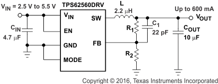
Typical Application Schematic

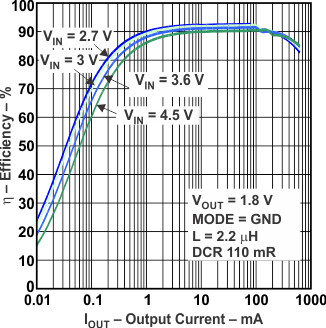
Efficiency vs Output Current

4 Revision History
Changes from C Revision (December 2009) to D Revision
- Added ESD Ratings table, Feature Description section, Device Functional Modes, Application and Implementation section, Power Supply Recommendations section, Layout section, Device and Documentation Support section, and Mechanical, Packaging, and Orderable Information section.Go
- Removed Ordering Information table Go
- Changed text string From ".....up to 1000-mA output current.." To ".....up to 600-mA output current.." in Description.Go
- Corrected typographical errors in Figure 32; from "VIN= 2 V to 6 V" to "VIN = 2.5 V to 5.5 V"Go
Changes from B Revision (March 2009) to C Revision
- Deleted High Efficiency Step Down ConverterGo
- Deleted "Wide" from Features bulletGo
- Deleted "for Li-Ion Batteries With Extended Voltage Range" from Features Go
- Deleted "Adjustable and Fixed Output-Voltage Options" from FeaturesGo
- Deleted "2.25 MHz Fixed Frequency Operation" from FeaturesGo
- Deleted "Power Save Mode at Light Load Currents" from Features Go
- Deleted "Voltage Positioning at Light Loads" from FeaturesGo
- Deleted "Allows < 1-mm Solution Height" from FeaturesGo
- Changed Description to better reflect device capabilities and differences to TPS62260Go
Changes from A Revision (July 2008) to B Revision
- Added TPS62562 device number.Go
Changes from * Revision (January 2008) to A Revision
- Changed at all levels. Revision A is a complete rewrite of this data sheet.Go
5 Device Comparison Table
| Part Number | Package | Mode Pin | Output Voltage(1) | Device Marking(2) |
|---|---|---|---|---|
| TPS62560 | SON (6) | yes | Adjustable | CEY |
| TPS62561 | SOT (5) | forced PWM only | Adjustable | CVO |
| TPS62562 | SON (6) | yes | 1.8 V fixed | NXT |
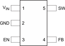
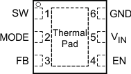
6 Pin Configuration and Functions


Pin Functions
| PIN | I/O | DESCRIPTION | ||
|---|---|---|---|---|
| NAME | No. QFN-6 |
No. TSOT23-5 |
||
| EN | 4 | 3 | I | This is the enable pin of the device. Pulling this pin to low forces the device into shutdown mode. Pulling this pin to high enables the device. This pin must be terminated. |
| FB | 3 | 4 | I | Feedback pin for the internal regulation loop. Connect the external resistor divider to this pin. In the fixed-output-voltage option, connect this terminal directly to the output capacitor. |
| GND | 6 | 2 | — | GND supply pin |
| MODE | 2 | N/A | I | This pin is only available as a QFN package option. MODE pin = high forces the device to operate in the fixed-frequency PWM mode. MODE pin = low enables the power-save mode with automatic transition from PFM mode to fixed-frequency PWM mode. |
| SW | 1 | 5 | O | This is the switch pin and is connected to the internal MOSFET switches. Connect the external inductor between this pin and the output capacitor. |
| VIN | 5 | 1 | — | VIN power-supply pin |
| Exposed Thermal Pad | — | N/A | — | Must be soldered to achieve appropriate power dissipation. Should be connected to GND. |