-
TPS6273x Step-Down Converter With Bypass Mode for Ultra Low-Power Wireless Applications
- 1 Features
- 2 Applications
- 3 Description
- 4 Revision History
- 5 Description (Continued)
- 6 Device Comparison Table
- 7 Pin Configuration and Functions
- 8 Specifications
- 9 Detailed Description
- 10Application and Implementation
- 11Power Supply Recommendations
- 12Layout
- 13Device and Documentation Support
- 14Mechanical, Packaging, and Orderable Information
- IMPORTANT NOTICE
Package Options
Mechanical Data (Package|Pins)
- DRY|6
Thermal pad, mechanical data (Package|Pins)
- DRY|6
Orderable Information
TPS6273x Step-Down Converter With Bypass Mode for Ultra Low-Power Wireless Applications
1 Features
- Input Voltage Range VIN From 1.9 V to 3.9 V
- Typ. 30-nA Ultra Low-Power Bypass Mode
- Typ. 25-μA DC-DC Quiescent Current
- Internal Feedback Divider Disconnect
- Typical 2.1-Ω Bypass Switch Between VIN and VOUT
- Automatic Transition from DC-DC to Bypass Mode
- Up to 3-MHz Switch Frequency
- Up to 95% DC-DC Efficiency
- Open-Drain Status Output STAT
- Output Peak Current up to 100 mA
- Fixed Output Voltages 1.9 V, 2.05 V, 2.1 V, 2.3 V
- Small External Output Filter Components 2.2 μH and 2.2 μF
- Optimized For Low Output Ripple Voltage
- Small 1 × 1.5 × 0.6-mm3 USON Package
- 12-mm2 Minimum Solution Size
2 Applications
- CC2540 Bluetooth™ Low-Energy
System-On-Chip Solution - Low-Power Wireless Applications
- RF4CE, Metering
3 Description
The TPS62730 is a high frequency synchronous step-down DC-DC converter optimized for ultra low-power wireless applications. The device is optimized to supply TI's Low-Power Wireless sub 1-GHz and 2.4-GHz RF transceivers and System-On-Chip (SoC) solutions. The TPS62730 reduces the current consumption drawn from the battery during TX and RX mode by a high efficient step-down voltage conversion. The device provides an output current of up to 100 mA and allows the use of tiny and low-cost chip inductors and capacitors. With an input voltage range of 1.9 V to 3.9 V, the device supports Li-primary battery chemistries such as Li-SOCl2, Li-SO2, Li-MnO2, and also two cell alkaline batteries.
The TPS62730 features an Ultra Low-Power bypass mode with typical 30-nA current consumption to support sleep and low power modes of TI's CC2540 Bluetooth Low Energy and CC430 SoC solutions. In this bypass mode, the output capacitor of the DC-DC converter is connected through an integrated typical 2.1-Ω bypass switch to the battery.
Device Information(1)
| PART NUMBER | PACKAGE | BODY SIZE (NOM) |
|---|---|---|
| TPS62730 | USON (6) | 1.45 mm x 1.00 mm |
| TPS62732 | ||
| TPS62733 |
- For all available packages, see the orderable addendum at the end of the datasheet.
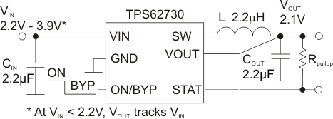
Typical Application

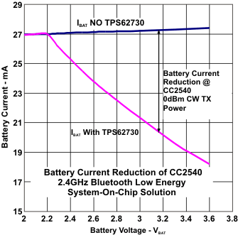
Battery Current Reduction Using TPS62730

4 Revision History
Changes from C Revision (December 2012) to D Revision
- Added Pin Configuration and Functions section, ESD Ratings table, Feature Description section, Device Functional Modes, Application and Implementation section, Power Supply Recommendations section, Layout section, Device and Documentation Support section, and Mechanical, Packaging, and Orderable Information section Go
5 Description (Continued)
In DC-DC operation mode the device provides a fixed output voltage to the system. With a switch frequency up to 3 MHz, the TPS62730 features low output ripple voltage and low noise even with a small 2.2-uF output capacitor. The automatic transition into bypass mode during DC-DC operation prevents an increase of output ripple voltage and noise once the DC-DC converter operates close to 100% duty cycle. The device automatically enters bypass mode once the battery voltage falls below the transition threshold VIT BYP . The TPS62730 is available in a 1 × 1.5-mm2 6-pin USON package.
6 Device Comparison Table
| TA | PART NUMBER | OUTPUT VOLTAGE [V] | AUTOMATIC BYPASS MODE TRANSITION THRESHOLDS VIT BYP | ||
|---|---|---|---|---|---|
| VIT BYP [V] RISING VIN | VIT BYP [V] FALLING VIN | VIT BYP [mV] HYSTERESIS | |||
| –40°C to 85°C | TPS62730 | 2.10 | 2.25 | 2.20 | 50 |
| TPS62731 (1) | 2.05 | 2.2 | 2.15 | 50 | |
| TPS62732 | 1.90 | 2.10 | 2.05 | 50 | |
| TPS62733 | 2.3 | 2.48 | 2.41 | 70 | |
| TPS62734 (1) | 2.10 | 2.28 | 2.23 | 50 | |
| TPS62735 (1) | 2.10 | 2.33 | 2.23 | 100 | |