-
TPS631000 1.5-A Output Current, High Power Density Buck-Boost Converter
- 1 Features
- 2 Applications
- 3 Description
- 4 Revision History
- 5 Pin Configuration and Functions
- 6 Specifications
- 7 Detailed Description
- 8 Application and Implementation
- 9 Power Supply Recommendations
- 10Layout
- 11Device and Documentation Support
- 12Mechanical, Packaging, and Orderable Information
- IMPORTANT NOTICE
Package Options
Mechanical Data (Package|Pins)
- DRL|8
Thermal pad, mechanical data (Package|Pins)
Orderable Information
TPS631000 1.5-A Output Current, High Power Density Buck-Boost Converter
1 Features
- 1.6-V to 5.5-V input voltage range
- Device input voltage > 1.65 V for start-up
- 1.2-V to 5.3-V output voltage range (adjustable)
- High output current capability, 3-A peak switch current
- 2-A output current for VIN ≥ 3 V, VOUT = 3.3 V
- 1.5-A output current for VIN ≥ 2.7 V, VOUT = 3.3 V
- High efficiency over the entire load range
- 8-μA typical quiescent current
- Power save mode
- 150-mV load-step response at a 1-A current step
- Peak current buck-boost mode architecture
- Seamless mode transition with < 20-mV output ripple
- Forward and reverse current operation
- Start-up into pre-biased outputs
- Fixed-frequency operation with 2-MHz switching
- Safety and robust operation features
- Overcurrent protection and short-circuit protection
- Integrated soft start with active ramp adoption
- Overtemperature protection and overvoltage protection
- True shutdown function with load disconnect
- Forward and backward current limit
- Small solution size
- Small 1-µH inductor
- Works with one 0805 output capacitor over the full VOUT range
- Create a custom design using the TPS631000 with the WEBENCH® Power Designer
2 Applications
- System pre-regulator (smartphone, tablet, terminal, telematics)
- Point-of-load regulation (wired sensor, port/cable adapter, and dongle)
- Fingerprint, camera sensors (electronic smart lock, IP network camera)
- RF amplifier supply (smart sensors)
- Voltage stabilizer (datacom, optical modules, cooling/heating)
3 Description
The TPS631000 is a constant frequency peak current mode control buck-boost converter. The device has a 3-A peak current limit (typical) and 1.6-V to 5.5-V input voltage range. The TPS631000 provides a power supply solution for system pre-regulators and voltage stabilizers.
Depending on the input voltage, the TPS631000 automatically operates in boost, buck, or in 3-cycle buck-boost mode when the input voltage is approximately equal to the output voltage. The transitions between modes happen at a defined duty cycle and avoid unwanted toggling within the modes to reduce output voltage ripple. 8-μA quiescent current and power save mode power enable the highest efficiency for light to no-load conditions.
The TPS631000 offers a very small solution size with a 1.2-mm × 2.1-mm SOT-583 package, a 1-μH inductor, and one 0805 output capacitor.
| PART NUMBER | PACKAGE(1) | BODY SIZE (NOM) |
|---|---|---|
| TPS631000 | SOT-583 | 1.6 mm × 2.1 mm |
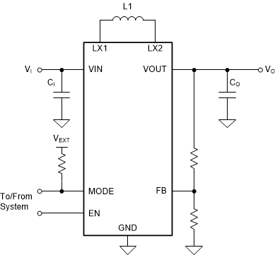
 Typical Application
5 Pin Configuration and Functions
| PIN | I/O(1) | DESCRIPTION | |
|---|---|---|---|
| NAME | NO. | ||
| VOUT | 1 | PWR | Power stage output |
| LX2 | 2 | PWR | Inductor switching node of the boost stage |
| LX1 | 3 | PWR | Inductor switching node of the buck stage |
| VIN | 4 | PWR | Supply input voltage |
| EN | 5 | I | Device enable. Set High to enable and Low to disable. It must not be left floating. |
| MODE | 6 | I | PFM/PWM selection. Set Low for power save mode, set High for forced PWM. It must not be left floating. |
| GND | 7 | PWR | Power ground |
| FB | 8 | I | Voltage feedback. Sensing pin |