-
TPS65295 complete DDR4 memory power solution
- 1 Features
- 2 Applications
- 3 Description
- 4 Revision History
- 5 Pin Configuration and Functions
- 6 Specifications
- 7 Detailed Description
- 8 Application and Implementation
- 9 Power Supply Recommendations
- 10Layout
- 11Device and Documentation Support
- 12Mechanical, Packaging, and Orderable Information
- IMPORTANT NOTICE
Package Options
Mechanical Data (Package|Pins)
- RJE|18
Thermal pad, mechanical data (Package|Pins)
Orderable Information
TPS65295 complete DDR4 memory power solution
1 Features
- Synchronous buck converter (VDDQ)
- Input voltage range: 4.5 V to 18 V
- Output voltage fixed at 1.2 V
- D-CAP3™ mode control for fast transient response
- Continual output current: 8 A
- Advanced Eco-mode™ pulse skip
- Integrated 22-mΩ and 8.6-mΩ RDS(on) internal power switch
- 600-kHz switching frequency
- Internal soft start: 1.6 ms
- Cycle-by-cycle overcurrent protection
- Latched output OV and UV protections
- Synchronous buck converter (VPP)
- Input voltage range: 3 V to 5.5 V
- Output voltage fixed at 2.5 V
- D-CAP3™ mode control for fast transient response
- Continual output current: 1 A
- Advanced Eco-mode™ pulse skip
- Integrated 150-mΩ and 120-mΩ RDS(on) internal power switch
- 580-kHz switching frequency
- Internal soft start: 1 ms
- Cycle-by-cycle overcurrent protection
- Latched output OV and UV protections
- 1-A LDO (VTT)
- 1-A continual sink and source current
- Requires only 10 μF of ceramic output capacitor
- Support high-z in S3
- ±30-mV VTT output accuracy (DC+AC)
- Buffered reference (VTTREF)
- Buffered, low noise, ±10-mA capability
- 0.8% output accuracy
- Low quiescent current: 150 µA
- Power good indicator
- Output discharge function
- Power up and power down sequencing control
- Non-latch for OT and UVLO protections
- 18-pin 3.0-mm × 3.0-mm HotRod™ VQFN package
2 Applications
- DDR4 memory power supplies
- Notebook, PC computers, and servers
- Ultrabook, tablet computers
- Single-board computer, computer on module
3 Description
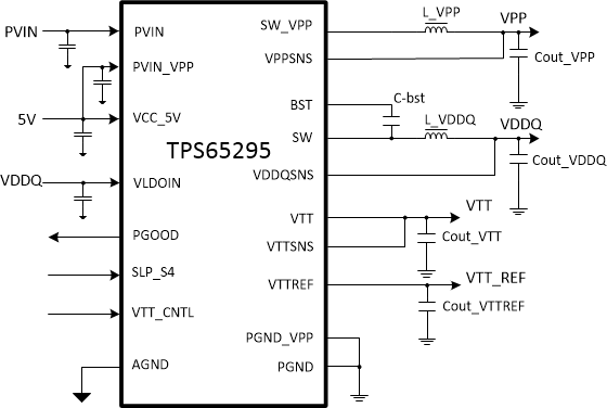
The TPS65295 device provides a complete power solution for DDR4 memory system with the lowest total cost and minimum space. It meets the JEDEC standard for DDR4 power-up and power-down sequence requirement. The TPS65295 integrates two synchronous buck converters (VPP and VDDQ) and a 1-A sink and source tracking LDO (VTT) and a buffered low noise reference (VTTREF). The TPS65295 employs D-CAP3™ mode coupled with 600-kHz switching frequency for ease-of-use, fast transient, and support for ceramic output capacitors without an external compensation circuit.
The VTTREF tracks ½ VDDQ within excellent 0.8% accuracy. The VTT, which provides both 1-A sink and source continual current capabilities, requires only 10-μF of ceramic output capacitor.
The TPS65295 provides rich functions as well as excellent power supply performance. It supports flexible power state control, placing VTT at high-Z in S3 and discharging VDDQ, VTT, and VTTREF in S4/S5 state. OVP, UVP, OCP, UVLO and thermal shutdown protections are also available. The part is available in a thermally enhanced 18-pin HotRod™ VQFN package and is designed to operate under the –40°C to 125°C junction temperature range.
Device Information(1)
| PART NUMBER | PACKAGE | BODY SIZE (NOM) |
|---|---|---|
| TPS65295 | VQFN (18) | 3.00 mm × 3.00 mm |
- For all available packages, see the orderable addendum at the end of the data sheet.
Typical Application

4 Revision History
| DATE | REVISION | NOTES |
|---|---|---|
| February 2019 | * | Initial release. |