SLVS915C February 2010 – July 2015 TPS73801
PRODUCTION DATA.
- 1 Features
- 2 Applications
- 3 Description
- 4 Revision History
- 5 Pin Configuration and Functions
- 6 Specifications
- 7 Detailed Description
- 8 Application and Implementation
- 9 Power Supply Recommendations
- 10Layout
- 11Device and Documentation Support
- 12Mechanical, Packaging, and Orderable Information
Package Options
Mechanical Data (Package|Pins)
- DCQ|6
Thermal pad, mechanical data (Package|Pins)
Orderable Information
1 Features
- Optimized for Fast Transient Response
- Output Current: 1.0 A
- Dropout Voltage: 300 mV
- Low Noise: 45 µVRMS (10 Hz to 100 kHz)
- 1-mA Quiescent Current
- No Protection Diodes Needed
- Controlled Quiescent Current in Dropout
- Adjustable Output Voltage: 1.21 to 20 V
- Less Than 1-µA Quiescent Current in Shutdown
- Stable With 10-µF Output Capacitor
- Stable With Ceramic Capacitors
- Reverse-Battery Protection
- No Reverse Current
- Thermal Limiting
2 Applications
- 3.3-V to 2.5-V Logic Power Supplies
- Post Regulator for Switching Supplies
- Portable/Battery-Powered Equipment.
3 Description
The TPS73801 is a low-dropout (LDO) regulator optimized for fast transient response. The device can supply 1.0 A of output current with a dropout voltage of 300 mV. Operating quiescent current is 1 mA, dropping to less than 1 µA in shutdown. Quiescent current is well controlled; it does not rise in dropout as it does with many other regulators. In addition to fast transient response, the TPS73801 regulators have very low output noise, which makes them ideal for sensitive RF supply applications.
Output voltage range is from 1.21 to 20 V. The TPS73801 regulators are stable with output capacitors as low as 10 µF. Small ceramic capacitors can be used without the necessary addition of ESR, as is common with other regulators. Internal protection circuitry includes reverse-battery protection, current limiting, thermal limiting, and reverse-current protection. The devices are available as an adjustable device with a 1.21-V reference voltage. The TPS73801 regulators are available in the 6-pin TO-223 (DCQ) packages.
Device Information(1)
| PART NUMBER | PACKAGE | BODY SIZE (NOM) |
|---|---|---|
| TPS73801 | SOT-223 (6) | 6.50 mm x 3.50 mm |
- For all available packages, see the orderable addendum at the end of the data sheet.
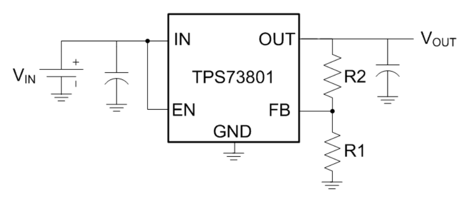
Simplified Schematic
