TPS7A8101-Q1 Low-Noise, Wide-Bandwidth, High PSRR, Low-Dropout 1-A Linear Regulator
1 Features
- Qualified for Automotive Applications
- AEC-Q100 Qualified With the Following Results:
- Device Temperature Grade 1: –40°C to 125°C Ambient Operating Temperature Range
- Device HBM ESD Classification Level H2
- Device CDM ESD Classification Level C4B
- Low-Dropout 1-A Regulator with Enable
- Adjustable Output Voltage: 0.8 V to 6 V
- Wide-Bandwidth High PSRR:
- 80 dB at 1 kHz
- 60 dB at 100 kHz
- 54 dB at 1 MHz
- Low Noise: 23.5 μVRMS typical (100 Hz to
100 kHz) - Stable With 4.7-μF Output Capacitance
- Excellent Load and Line Transient Response
- 3% Overall Accuracy (Over Load, Line, Temperature)
- Over-Current and Overtemperature Protection
- Very Low Dropout: 170 mV Typical at 1 A
- Package: 3-mm × 3-mm SON-8
2 Applications
- RF Power in Automotive Applications
- Automotive ADAS ECUs
- Telematic Control Units
- Audio
- High-Speed I/F (PLL and VCO)
3 Description
The TPS7A8101-Q1 low-dropout linear regulator (LDO) offers very good performance in output noise and power-supply rejection ratio (PSRR). This LDO uses an advanced BiCMOS process and a PMOSFET pass device to achieve very low noise, excellent transient response, and excellent PSRR performance.
The TPS7A8101-Q1 device is stable with a 4.7-μF ceramic output capacitor and uses a precision voltage reference and feedback loop to achieve a worst-case accuracy of 3% over all load, line, process, and temperature variations.
This device is fully specified over the temperature range of TA = –40°C to 125°C and is offered in a
3-mm × 3-mm, SON-8 package with a thermal pad.
Device Information(1)
| PART NUMBER | PACKAGE | BODY SIZE (NOM) |
|---|---|---|
| TPS7A8101-Q1 | SON (8) | 3.00 mm × 3.00 mm |
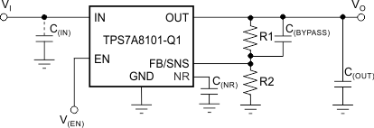
4 Typical Application Circuit
Typical Power-Supply Ripple Rejection

5 Revision History
Changes from * Revision (April 2014) to A Revision
- Changed device status from Product Preview to Production DataGo
6 Pin Configuration and Functions

Pin Functions
| PIN | DESCRIPTION | |
|---|---|---|
| NAME | NO. | |
| EN | 5 | Driving this pin high turns on the regulator. Driving this pin low puts the regulator into shutdown mode. See to the Shutdown section for more details. The EN pin must not be left floating and can be connected to the IN pin if not used. |
| FB/SNS | 3 | This pin is the input to the error amplifier and is used to set the output voltage of the device. |
| GND | 4 | Ground |
| IN | 7 | Unregulated input supply |
| 8 | ||
| NR | 6 | Connect an external capacitor between this pin and ground to reduce output noise to very low levels. The capacitor also slows down the VO ramp (RC soft start). |
| OUT | 1 | Regulator output. A 4.7-μF or larger ceramic capacitor is required for stability. |
| 2 | ||
| Thermal Pad | — | The Thermal Pad should be connected to GND. |
7 Specifications
7.1 Absolute Maximum Ratings
Over operating free-air temperature range (unless otherwise noted).(1)| MIN | MAX | UNIT | ||
|---|---|---|---|---|
| Voltage | IN | –0.3 | 7 | V |
| FB/SNS, NR | –0.3 | 3.6 | V | |
| EN | –0.3 | VI + 0.3(2) | V | |
| OUT | –0.3 | 7 | V | |
| Current | OUT | Internally Limited | A | |
| Operating junction temperature, TJ | –55 | 150 | °C | |
7.2 Handling Ratings
| MIN | MAX | UNIT | ||||
|---|---|---|---|---|---|---|
| Tstg | Storage temperature range | –55 | 150 | °C | ||
| V(ESD) | Electrostatic discharge | Human body model (HBM), per AEC Q100-002, classification level H2(1) | –2 | 2 | kV | |
| Charged device model (CDM), per JEDEC specification JESD22-C101, classification level C4B | Corner pins (1, 4, 5, and 8) |
–750 | 750 | V | ||
| Other pins | –500 | 500 | ||||
7.3 Recommended Operating Conditions
Over operating free-air temperature range (unless otherwise noted)| MIN | MAX | UNIT | ||
|---|---|---|---|---|
| VI | Input voltage | 2.2 | 6.5 | V |
| IO | Output current | 0 | 1 | A |
| TA | Operating free air temperature | –40 | 125 | °C |
7.4 Thermal Information
| THERMAL METRIC(1) | DRB | UNIT | |
|---|---|---|---|
| (8 PINS) | |||
| RθJA | Junction-to-ambient thermal resistance | 45.7 | °C/W |
| RθJC(top) | Junction-to-case (top) thermal resistance | 53.1 | |
| RθJB | Junction-to-board thermal resistance | 21.2 | |
| ψJT | Junction-to-top characterization parameter | 0.9 | |
| ψJB | Junction-to-board characterization parameter | 21.4 | |
| RθJC(bot) | Junction-to-case (bottom) thermal resistance | 5.2 | |
7.5 Electrical Characteristics
Over the temperature range of –40°C ≤ TA, TJ ≤ 125°C, VI = VOnom + 0.5 V or 2.2 V (whichever is greater), IO = 1 mA, V(EN) = 2.2 V, C(OUT) = 4.7 μF, C(NR) = 0.01 μF, and C(BYPASS) = 0 μF, unless otherwise noted. The device is tested at VO = 0.8 V and VO = 6 V. Typical values are at TJ = 25°C.| PARAMETER | TEST CONDITIONS | MIN | TYP | MAX | UNIT | |||
|---|---|---|---|---|---|---|---|---|
| VI | Input voltage range(1) | 2.2 | 6.5 | V | ||||
| V(NR) | Internal reference | 0.79 | 0.8 | 0.81 | V | |||
| VO | Output voltage range | 0.8 | 6 | V | ||||
| Output accuracy(2) | VO + 0.5 V ≤ VI ≤ 6 V, VI ≥ 2.5 V, 100 mA ≤ IO ≤ 500 mA, 0°C ≤ TJ ≤ 85°C |
–2% | 2% | |||||
| VO + 0.5 V ≤ VI ≤ 6.5 V, VI ≥ 2.2 V, 100 mA ≤ IO ≤ 1 A |
–3% | ±0.3% | 3% | |||||
| ΔVO(ΔVI) | Line regulation | VOnom + 0.5 V ≤ VI ≤ 6.5 V, VI ≥ 2.2 V, IO = 100 mA |
150 | μV/V | ||||
| ΔVO(ΔIL) | Load regulation | 100 mA ≤ IO ≤ 1 A | 2 | μV/mA | ||||
| VDO | Dropout voltage(3) | VO + 0.5 V ≤ VI ≤ 6.5 V, VI ≥ 2.2 V, IO = 500 mA, V(FB/SNS) = GND |
250 | mV | ||||
| VO + 0.5 V ≤ VI ≤ 6.5 V, VI ≥ 2.5 V, IO = 750 mA, V(FB/SNS) = GND |
350 | mV | ||||||
| VO + 0.5 V ≤ VI ≤ 6.5 V, VI ≥ 2.5 V, IO = 1 A, V(FB/SNS) = GND |
500 | mV | ||||||
| IL | Output current-limit | VO = 0.85 × VOnom, VI ≥ 3.3 V | 1100 | 1400 | 2000 | mA | ||
| I(GND) | Ground pin current | IO = 1 mA | 60 | 100 | μA | |||
| IO = 1 A | 350 | μA | ||||||
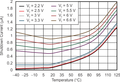
| IL(sd) | Shutdown current (I(GND)) | V(EN) ≤ 0.4 V, VI ≥ 2.2 V, RL = 1 kΩ, 0°C ≤ TJ ≤ 125°C |
0.2 | 2.5 | μA | |||
| I(FB/SNS) | Feedback pin current | VI = 6.5 V, V(FB/SNS) = 0.8 V | 0.02 | 1 | μA | |||
| PSRR | Power-supply rejection ratio | VI = 4.3 V, VO = 3.3 V, IO = 750 mA |
ƒ = 100 Hz | 80 | dB | |||
| ƒ = 1 kHz | 82 | dB | ||||||
| ƒ = 10 kHz | 78 | dB | ||||||
| ƒ = 100 kHz | 60 | dB | ||||||
| ƒ = 1 MHz | 54 | dB | ||||||
| Vn | Output noise voltage | BW = 100 Hz to 100 kHz, VI = 3.8 V, VO = 3.3 V, IO = 100 mA, C(NR) = C(BYPASS) = 470 nF |
23.5 | μVRMS | ||||
| V(EN)H | Enable high (enabled) | 2.2 V ≤ VI ≤ 3.6 V, RL = 1 kΩ | 1.2 | V | ||||
| 3.6 V < VI ≤ 6.5 V, RL = 1 kΩ | 1.35 | V | ||||||
| V(EN)L | Enable low (shutdown) | RL = 1 kΩ | 0 | 0.4 | V | |||
| I(EN) | Enable pin current, enabled | VI = V(EN) = 6.5 V | 0.02 | 1 | μA | |||
| tst | Startup time | VOnom = 3.3 V, VO = 0% to 90% VOnom, R1 = 3.3 kΩ, C(OUT) = 10 μF, C(NR) = 470 nF |
80 | ms | ||||
| UVLO | Undervoltage lockout | VI rising, RL = 1 kΩ | 1.86 | 2 | 2.1 | V | ||
| Hysteresis | VI falling, RL = 1 kΩ | 75 | mV | |||||
| Tsd | Thermal shutdown temperature | Shutdown, temperature increasing | 160 | °C | ||||
| Reset, temperature decreasing | 140 | °C | ||||||
7.6 Typical Characteristics
At VOnom = 3.3 V, VI = VOnom + 0.5 V or 2.2 V (whichever is greater), IO = 100 mA, V(EN) = VI, C(IN) = 1 μF, C(OUT) = 4.7 μF, and C(NR) = 0.01 μF; all temperature values refer to TJ, unless otherwise noted.
| NOTE: The Y-axis shows 1% VO per division | ||

| VO = 0.8 V | IO = 750 mA | |
| NOTE: The Y-axis shows 1% VO per division | ||

| IO = 1 A | ||

| IO = 500 mA | ||

| VI = 3.6 V | ||


| VO = VI – 0.5 V |

| VI – VO = 1 V | C(IN) = 0 F | C(OUT) = 10 µF |
| C(NR) = C(BYPASS) = 470 nF | ||

| VI – VO = 1 V | C(IN) = 0 F | C(OUT) = 10 µF |
| C(NR) = C(BYPASS) = 470 nF | ||

| IO = 100 mA | C(IN) = 0 F |

| VI – VO = 0.5 V | C(OUT) = 10 µF | C(IN) = 10 µF | |
| 24.09 µVRMS (C(NR) = C(BYPASS) = 100 nF) | |||
| 23.54 µVRMS (C(NR) = C(BYPASS) = 470 nF) | |||

| 23.54 µVRMS (IO = 100 mA) | C(IN) = 10 µF | VI – VO = 0.5 V |
| 23.71 µVRMS (IO = 750 mA) | C(NR) = 470 nF | C(OUT) = 10 µF |
| 22.78 µVRMS (IO = 1 A) | C(BYPASS) = 470 nF | |

| Using the same value of C(NR) and C(BYPASS) in the X-Axis |

| IO = 100 mA → 1 A → 100 mA | ||

| RL = 33 Ω | C(NR) = 470 nF | C(BYPASS) = 470 nF | ||
| C(OUT) = 10 µF | C(IN) = 10 µF | |||
| (1) The internal reference requires approximately 80 ms of rampup time (see Startup) from the enable event; therefore, VO fully reaches the target output voltage of 3.3 V in 80 ms from startup. | ||||

| NOTE: The Y-axis shows 1% VO per division | ||

| VO = 0.8 V | IO = 5 mA | |
| NOTE: The Y-axis shows 1% VO per division | ||

| IO = 750 mA | ||

| VI = 3.6 V | ||

| VO = 0.8 V | IO = 750 mA | |
| V(EN) = 0.4 V | ||

| C(NR) = C(BYPASS) = 470 nF | C(OUT) = 10 µF | C(IN) = 0 F |

| VI – VO = 0.5 V | C(IN) = 0 F | C(OUT) = 10 µF |
| C(NR) = C(BYPASS) = 470 nF | ||

| VI – VO = 0.5 V | C(IN) = 0 F | C(OUT) = 10 µF |
| C(NR) = C(BYPASS) = 470 nF | ||

| IO = 750 mA | C(IN) = 0 F |

| 25.89 µVRMS (VO = 1.8 V) | C(IN) = 10 µF | VI – VO = 0.5 V |
| 23.54 µVRMS (VO = 2.5 V) | C(NR) = 470 nF | C(OUT) = 10 µF |
| 23.54 µVRMS (VO = 3.3 V) | C(BYPASS) = 470 nF | |

| 23.54 µVRMS (CO = 10 µF) | C(IN) = 10 µF | VI – VO = 0.5 V |
| 23.91 µVRMS (CO = 22 µF) | C(NR) = 470 nF | C(OUT) = 10 µF |
| 22.78 µVRMS (CO = 100 µF) | C(BYPASS) = 470 nF | |

| VI = 3.8 V → 4.8 V → 3.8 V | ||
| IO = 500 mA | ||

| RL = 33 Ω | C(NR) = 470 nF | C(BYPASS) = 470 nF |
| C(OUT) = 10 µF | C(IN) = 10 µF |
8 Detailed Description
8.1 Overview
The TPS7A8101-Q1 device belongs to a family of new-generation LDO regulators that use innovative circuitry to achieve wide bandwidth and high loop gain, resulting in extremely high PSRR (over a 1-MHz range) even with very low headroom (VI – VO). A noise-reduction capacitor (C(NR)) at the NR pin and a bypass capacitor (C(BYPASS)) decrease noise generated by the bandgap reference in order to improve PSRR, while a quick-start circuit fast-charges the noise-reduction capacitor. This family of regulators offers sub-bandgap output voltages, current-limit, and thermal protection, and is fully specified from –40°C to 125°C.
8.2 Functional Block Diagram
 Figure 30. Functional Block Diagram
8.3 Feature Description
8.3.1 Internal Current-Limit
The TPS7A8101-Q1 internal current-limit helps protect the regulator during fault conditions. During the current-limit, the output sources a fixed amount of current that is largely independent of the output voltage. For reliable operation, the device should not be operated in a current-limit state for extended periods of time.
The PMOS pass element in the TPS7A8101-Q1 device has a built-in body diode that conducts current when the voltage at the OUT pin (V(OUT)) exceeds the voltage at the IN pin (V(IN)). This current is not limited, so if extended reverse-voltage operation is anticipated, external limiting may be appropriate.
8.3.2 Shutdown
The enable pin (EN) is active high and is compatible with standard-voltage and low-voltage TTL-CMOS levels. When shutdown capability is not required, the EN pin can connect to the IN pin.
8.3.3 Startup
Through a lower resistance, the bandgap reference can quickly charge the noise-reduction capacitor (C(NR)). The TPS7A8101-Q1 device has a quick-start circuit to quickly charge C(NR), if present; see Figure 30. At startup, this quick-start switch is closed, with only 33 kΩ of resistance between the bandgap reference and the NR pin. The quick-start switch opens approximately 100 ms after any device-enabling event, and the resistance between the bandgap reference and the NR pin becomes higher in value (approximately 250 kΩ) to form a very-good low-pass (RC) filter. This low-pass filter reduces the noise present on the reference voltage; therefore, reducing the noise on the output.
Inrush current can cause problems in many applications. The 33-kΩ resistance during the startup period is intentionally placed between the bandgap reference and the NR pin in order to slow down the reference voltage rampup, thus reducing the inrush current.
Use Equation 1 to calculate the startup time with other C(NR) values. For example, the capacitance of connecting the recommended C(NR) value of 0.47 μF along with the 33-kΩ resistance causes an 80-ms RC delay (approximately).
Although the noise-reduction effect is nearly saturated at 0.47 μF, connecting a C(NR) value greater than 0.47 μF can additionally help reduce noise. However, when connecting a C(NR) value greater than 0.47 µF, the startup time is extremely long because the quick-start switch opens after approximately 100 ms. That is, if C(NR) is not fully charged during this 100-ms period, C(NR) finishes charging through a higher resistance of 250 kΩ, and takes much longer to fully charge.
NOTE
A low-leakage capacitor should be used for C(NR). Most ceramic capacitors are suitable
8.3.4 Undervoltage Lockout (UVLO)
The TPS7A8101-Q1 device uses an undervoltage-lockout (UVLO) circuit to ensure that the output is shut off until the internal circuitry has enough voltage to operate properly. The UVLO circuit has a deglitch feature so that the circuit typically ignores undershoot transients on the input if the duration is less than 50-μs.
8.4 Device Functional Modes
Driving the EN pin over 1.2 V for VI between 2.2 V to 3.6 V or 1.35 V for VI between 3.6 V and 6.5 V turns on the regulator. Driving the EN pin below 0.4 V causes the regulator to enter shutdown mode.
In shutdown, the current consumption of the device is reduced to 0.02 µA typically.
