TPS7B69xx-Q1 High-Voltage Ultra-Low IQ Low-Dropout Regulator
1 Features
- Qualified for Automotive Applications
- AEC-Q100 Qualified With the Following Results:
- Device Temperature Grade 1: –40°C to 125°C Ambient Operating Temperature Range
- Device HBM ESD Classification Level 2
- Device CDM ESD Classification Level C4B
- 4 to 40-V Wide VI Input Voltage Range With up to 45-V Transient
- Maximum Output Current: 150 mA
- Low Quiescent Current (IQ):
- 15 µA Typical at Light Loads
- 25 µA Maximum Under Full Temperature
- 450-mV Typical Low Dropout Voltage at 100 mA Load Current
- Stable With Low ESR Ceramic Output Capacitor (2.2 to 100 µF)
- Fixed 2.5-V, 3.3-V, and 5-V Output Voltage Options
- Integrated Fault Protection:
- Thermal Shutdown
- Short-Circuit Protection
- Packages:
- 4-Pin SOT-223 Package
- 5-Pin SOT-23 Package
2 Applications
- Automotive
- Infotainment Systems With Sleep Mode
- Always-On Battery Applications
- Door Modules
- Remote Keyless-Entry Systems
- Immobilizers
3 Description
The TPS7B69xx-Q1 device is a low-dropout linear regulator designed for up to 40-V VI operations. With only 15-µA (typical) quiescent current at light load, the device is suitable for standby microcontrol-unit systems especially in automotive applications.
The devices feature an integrated short-circuit and overcurrent protection. The TPS7B69xx-Q1 device operates over a –40°C to 125°C temperature range. Because of these features, the TPS7B6925-Q1, TPS7B6933-Q1, and TPS7B6950-Q1 devices are well suited in power supplies for various automotive applications.
Device Information(1)
| PART NUMBER | PACKAGE | BODY SIZE (NOM) |
|---|---|---|
| TPS7B6925-Q1 TPS7B6933-Q1 TPS7B6950-Q1 |
SOT-223 (4) | 6.50 mm × 3.50 mm |
| SOT-23 (5) | 2.90 mm × 1.60 mm |
- For all available packages, see the orderable addendum at the end of the datasheet.
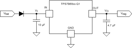
4 Typical Application Schematic
5 Revision History
Changes from A Revision (December 2014) to B Revision
- Changed the TPS7B6933-Q1 device status from Product Preview to Production DataGo
- Added the TPS7B6933-Q1 device test results to the Typical Characteristics section Go
Changes from * Revision (November 2014) to A Revision
- Changed the device status from Product Preview to Production DataGo
6 Pin Configuration and Functions


Pin Functions
| PIN | TYPE | DESCRIPTION | ||
|---|---|---|---|---|
| NAME | NO. | |||
| SOT-223 | SOT-23 | |||
| GND | 2 | 3 | G | Ground reference |
| 4 | 4 | |||
| IN | 1 | 1 | P | Input power-supply voltage |
| NC | — | 2 | — | Not connected pin |
| OUT | 3 | 5 | P | Output voltage |
7 Specifications
7.1 Absolute Maximum Ratings
over operating free-air temperature range (unless otherwise noted)(1)| MIN | MAX | UNIT | ||
|---|---|---|---|---|
| Unregulated input voltage | IN(2)(3)(4) | –0.3 | 45 | V |
| Regulated output voltage | OUT(2)(3) | –0.3 | 7 | V |
| Operating junction temperature range, TJ | –40 | 150 | °C | |
| Storage temperature, Tstg | –65 | 150 | °C | |
7.2 ESD Ratings
| VALUE | UNIT | ||||
|---|---|---|---|---|---|
| V(ESD) | Electrostatic discharge | Human body model (HBM), per AEC Q100-002(1) | ±2000 | V | |
| Charged device model (CDM), per AEC Q100-011 | Other pins | ±500 | |||
| Corner pins (4 pin: 1, 3, and 4; 5 pin: 1, 3, 4, and 5) |
±750 | ||||
7.3 Recommended Operating Conditions
over operating free-air temperature range (unless otherwise noted)| MIN | MAX | UNIT | ||
|---|---|---|---|---|
| VI | Unregulated input voltage | 4 | 40 | V |
| VO | Output voltage | 0 | 5.5 | V |
| CO | Output capacitor requirements(1) | 2.2 | 100 | µF |
| ESRCO | Output ESR requirements(2) | 0.001 | 2 | Ω |
| TJ | Operating junction temperature range | –40 | 150 | °C |
7.4 Thermal Information
| THERMAL METRIC(1)(2) | DCY | DBV | UNIT | |
|---|---|---|---|---|
| 4 PINS | 5 PINS | |||
| RθJA | Junction-to-ambient thermal resistance | 64.2 | 210.4 | °C/W |
| RθJC(top) | Junction-to-case (top) thermal resistance | 46.8 | 126.1 | |
| RθJB | Junction-to-board thermal resistance | 13.3 | 38.4 | |
| ψJT | Junction-to-top characterization parameter | 6.3 | 16 | |
| ψJB | Junction-to-board characterization parameter | 13.2 | 37.5 | |
7.5 Electrical Characteristics
VIN = 14 V, 1 mΩ < ESR < 2 Ω, TJ = –40°C to 150 °C (unless otherwise noted)| PARAMETER | TEST CONDITIONS | MIN | TYP | MAX | UNIT | |
|---|---|---|---|---|---|---|
| SUPPLY VOLTAGE AND CURRENT (IN) | ||||||
| VI | Input voltage | Fixed 2.5-V output, IO = 1 mA | 4 | 40 | V | |
| Fixed 3.3-V output, IO = 1 mA | 4 | 40 | ||||
| Fixed 5-V output, IO = 1 mA | 5.5 | 40 | ||||
| IQ | Quiescent current | Fixed 2.5-V and 3.3-V version, VI = 4 to 40 V, Fixed 5-V version, VI = 5.5 to 40 V, IO = 0.2 mA |
15 | 25 | µA | |
| VIN(UVLO) | IN undervoltage detection | Ramp VI up until the output turns on | 3.65 | V | ||
| Ramp VI down until the output turns OFF | 3 | |||||
| REGULATED OUTPUT (OUT) | ||||||
| VO | Regulated output | Fixed 2.5-V version, VI = 4 to 40 V, IO = 1 to 150 mA | –3% | 3% | ||
| Fixed 3.3-V version, VI = 5 to 40 V, IO = 1 to 150 mA | –3% | 3% | ||||
| Fixed 5-V version, VI = 6.5 to 40 V, IO = 1 to 150 mA | –3% | 3% | ||||
| ΔVO(ΔVI) | Line regulation | VI = 6 to 40 V, ∆VO, IO = 10 mA | 10 | mV | ||
| ΔVO(ΔIL) | Load regulation | IO = 1 to 150 mA, ∆VO | 20 | mV | ||
| VDROP | Dropout voltage | Fixed 2.5-V version, VI – VO, IO = 50 mA | 1.575 | V | ||
| Fixed 2.5-V version, VI – VO, IO = 100 mA | 1.575 | |||||
| Fixed 3.3-V version, VI – VO, IO = 50 mA | 799 | mV | ||||
| Fixed 3.3-V version, VI – VO, IO = 100 mA | 800 | |||||
| Fixed 5-V version, VI – VO, IO = 50 mA | 220 | 400 | ||||
| Fixed 5-V version, VI – VO, IO = 100 mA | 450 | 800 | ||||
| IO | Output current | VO in regulation | 0 | 150 | mA | |
| IOCL | Output current-limit | OUT short to ground | 150 | 500 | mA | |
| PSRR | Power supply ripple rejection(1) | Vrip = 0.5 Vpp, Load = 10 mA, ƒ = 100 Hz, CO = 2.2 µF | 60 | dB | ||
| OPERATING TEMPERATURE RANGE | ||||||
| Tsd | Junction shutdown temperature | 175 | °C | |||
| Thys | Hysteresis of thermal shutdown | 25 | °C | |||
7.6 Typical Characteristics


| VI = 14 V | ||

| IO = 0 mA | ||


| IO = 10 mA | VI = 14 V | TA = 25°C |
| CO = 2.2 µF |

| VI = 14 V | CO = 2.2 µF | 1 ms/div |
| VO = 5 V | ||

| VI = 14 V | CO = 2.2 µF | 1 ms/div |
| VO = 2.5 V | ||

| VI = 14 V | CO = 2.2 µF | 1 ms/div |
| VO = 3.3 V | ||

| VI = 9 to 16 V | CO = 2.2 µF | 1 ms/div |
| IO = 10 mA | ||

| VI = 9 to 16 V | CO = 2.2 µF | 1 ms/div |
| IO = 10 mA | ||

| CO = 2.2 µF, 400 µs/div | ||


| IO = 0 mA | ||

| IO = 0 mA | ||

| IO = 0.2 mA | ||

| IO = 100 mA | VI = 14 V | TA = 25°C |
| CO = 2.2 µF |


| VI = 14 V | CO = 2.2 µF | 1 ms/div |
| VO = 3.3 V | ||

| VI = 14 V | CO = 2.2 µF | 1 ms/div |
| VO = 5 V | ||

| VI = 14 V | CO = 2.2 µF | 1 ms/div |
| VO = 2.5 V |

| VI = 9 to 16 V | CO = 2.2 µF | 1 ms/div |
| IO = 10 mA | ||

| CO = 2.2 µF, 400 µs/div | ||

| CO = 2.2 µF, 400 µs/div | ||
8 Detailed Description
8.1 Overview
The TPS7B69xx-Q1 high-voltage linear regulator operates over a 4-V to 40-V input voltage range. The device has an output current capability of 150 mA and offers fixed output voltages of 2.5 V (TPS7B6925-Q1), 3.3 V (TPS7B6933-Q1) or 5 V (TPS7B6950-Q1). The device features a thermal shutdown and short-circuit protection to prevent damage during over-temperature and overcurrent conditions.
8.2 Functional Block Diagram

8.3 Feature Description
8.3.1 Input (IN)
The IN pin is a high-voltage-tolerant pin. A capacitor with a value higher than 0.1 µF is recommended to be connected close to this pin to better the transient performance.
8.3.2 Output (OUT)
The OUT pin is the regulated output based on the required voltage. The output has current limitation. During the initial power up, the regulator has a soft start incorporated to control the initial current through the pass element and the output capacitor.
In the event that the regulator drops out of regulation, the output tracks the input minus a drop based on the load current. When the input voltage drops below the UVLO threshold, the regulator shuts down until the input voltage recovers above the minimum startup level.
8.3.3 Output Capacitor Selection
For stable operation over the full temperature range and with load currents up to 150 mA, use a capacitor with an effective value between 2.2 µF and 100 µF and ESR smaller than 2 Ω. To better the load transient performance, an output capacitor, such as a ceramic capacitor with low ESR, is recommended.
8.3.4 Low-Voltage Tracking
At low input voltages, the regulator drops out of regulation and the output voltage tracks input minus a voltage based on the load current (IL) and switch resistor. This tracking allows for a smaller input capacitor and can possibly eliminate the need for a boost converter during cold-crank conditions.
8.3.5 Thermal Shutdown
The TPS7B69xx-Q1 family of devices incorporates a thermal-shutdown (TSD) circuit as a protection from overheating. For continuous normal operation, the junction temperature should not exceed the TSD trip point. If the junction temperature exceeds the TSD trip point, the output turns off. When the junction temperature falls below the TSD trip point minus the hysteresis of TSD, the output turns on again. This cycling limits the dissipation of the regulator, protecting it from damage as a result of overheating.
The purpose of the design of the internal protection circuitry of the TPS7B69xx-Q1 family of devices is for protection against overload conditions, not as a replacement for proper heat-sinking. Continuously running the TPS7B69xx-Q1 family of devices into thermal shutdown degrades device reliability.
8.4 Device Functional Modes
8.4.1 Operation With VI Less Than 4 V
The TPS7B69xx-Q1 family of devices operates with input voltages above 4 V. The maximum UVLO voltage is 3 V and the device operates at an input voltage above 4 V. The device can also operate at lower input voltages; no minimum UVLO voltage is specified. At input voltages below the actual UVLO, the device shuts down.
8.4.2 Operation With VI Greater Than 4 V
When VI is greater than 4 V, if the input voltage is higher than VO plus the dropout voltage, the output voltage is equal to the set value. Otherwise, the output voltage is equal to VI minus the dropout voltage.