TRF37x32 Dual Down Converter Mixer With Integrated IF AMP
1 Features
- Device Family Supports Wide RF Input Range
- TRF37A32: 400 - 1700 MHz
- TRF37B32: 700 - 2700 MHz
- TRF37C32: 1700 - 3800 MHz
- Gain: 10 dB
- Noise Figure: 9.5 dB
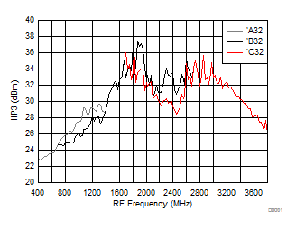
- Input IP3: 30 dBm
- 500 mW per Channel Power Dissipation
- Single Ended RF Input
- IF Frequency Range from 30 MHz to 600 MHz
- 45 dB Isolation between Channels
- Low Power Mode Option
- Independent Power Down Control
- Single 3.3V Supply
- No External Matching Required
2 Applications
- Wireless Infrastructure
- WCDMA, TD-SCDMA
- LTE, TD-LTE
- Multicarrier GSM (MC-GSM)
- Point-to-Point Microwave
- Software Defined Radios (SDR)
- Radar Receiver
- Satellite Communications
3 Description
The TRF37x32 is a wideband dual down converter mixer with integrated IF amplifier. The device employs integrated baluns for single ended RF and LO inputs. The IF amplifier operates from 30 MHz to 600 MHz in an open collector topology to support a variety of IF frequencies and bandwidths. The TRF37x32 provides excellent mixer linearity and noise performance and offers good isolation between channels for operation with diversity applications. The device operates with low power dissipation and further provides an option for a low power mode for power sensitive applications. Each channel can be independently powered down with fast response times to allow operation in time domain duplexed (TDD) applications.
Device Information(1)
| PART NUMBER | PACKAGE | BODY SIZE (NOM) |
|---|---|---|
| TRF37A32 | WQFN (32) | 5.00mm x 5.00mm |
| TRF37B32 | ||
| TRF37C32 |
- For all available packages, see the orderable addendum at the end of the datasheet.
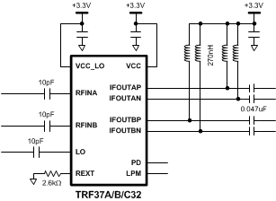
4 Simplified Schematic
IIP3 Performance Across Frequency
5 Revision History
Changes from * Revision (May 2014) to A Revision
- Added Typical Characteristics, Feature Description section, Device Functional Modes, Application and Implementation section, Power Supply Recommendations section, and Layout sectionGo
- Replaced the Handling Ratings table with the ESD Ratings tableGo
6 Pin Configuration and Functions
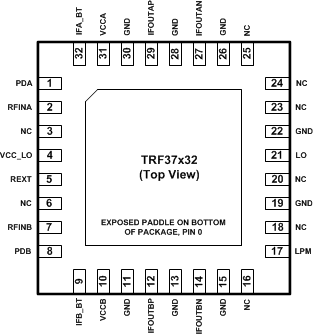
Pin Functions
| PIN | I/O | DESCRIPTION | |
|---|---|---|---|
| NAME | NO. | ||
| PDA | 1 | Digital Input | Power down for channel A (1 = PD; 0 or open = powered) |
| RFINA | 2 | Analog Input | RF input for channel A |
| NC | 3 | N/A | No connect |
| VCC_LO | 4 | Supply | VCC supply for the LO circuitry |
| REXT | 5 | Bias | External bias resistor |
| NC | 6 | N/A | No connect |
| RFINB | 7 | Analog Input | RF input for channel B |
| PDB | 8 | Digital Input | Power down for channel B (1 = PD; 0 or open = powered) |
| IFB_BT | 9 | N/A | IF channel B bias control; leave unconnected |
| VCCB | 10 | Supply | Power supply for channel B |
| GND | 11 | Ground | Ground |
| IFOUTBP | 12 | Analog Output | IF out channel B: positive |
| GND | 13 | Ground | Ground |
| IFOUTBN | 14 | Analog Output | IF out channel B: negative |
| GND | 15 | Ground | Ground |
| NC | 16 | N/A | No connect |
| LPM | 17 | Digital Input | Low power mode (0 = normal; 1 = low power) |
| NC | 18 | N/A | No connect |
| GND | 19 | Ground | Ground |
| NC | 20 | N/A | No connect |
| LO | 21 | Analog Input | Local oscillator (LO) input |
| GND | 22 | Ground | Ground |
| NC | 23 | N/A | No connect |
| NC | 24 | N/A | No connect |
| NC | 25 | N/A | No connect |
| GND | 26 | Ground | Ground |
| IFOUTAN | 27 | Analog Output | IF out channel A: negative |
| GND | 28 | Ground | Ground |
| IFOUTAP | 29 | Analog Output | IF out channel A: positive |
| GND | 30 | Ground | Ground |
| VCCA | 31 | Supply | Power supply for channel A |
| IFA_BT | 32 | N/A | IF channel A bias control; leave unconnected |