-
TS3USBA225 USB 2.0 High-Speed (480 Mbps) and Audio Switches with Negative Signal Capability and 1.8-V Logic Compatibility and Power-Down Mode
- 1 Features
- 2 Applications
- 3 Description
- 4 Revision History
- 5 Pin Configuration and Functions
- 6 Specifications
- 7 Detailed Description
- 8 Application and Implementation
- 9 Power Supply Recommendations
- 10Layout
- 11Device and Documentation Support
- 12Mechanical, Packaging, and Orderable Information
- IMPORTANT NOTICE
Package Options
Mechanical Data (Package|Pins)
- RUT|12
Thermal pad, mechanical data (Package|Pins)
Orderable Information
TS3USBA225 USB 2.0 High-Speed (480 Mbps) and Audio Switches with Negative Signal Capability and 1.8-V Logic Compatibility and Power-Down Mode
1 Features
- 2.7-V to 5.0-V Operating Power Supply (VCC)
- MHL/High-Speed USB (480 Mbps) Switch:
- V I/O Accepts Signals up to 4.5 V (Independent of VCC)
- 6.5 Ω rON Typical
- 3 pF CON Typical
- 1.9 GHz Bandwidth (–3 dB)
- Audio Switch:
- 1.8-V Compatible Control Input (SEL1 and SEL2) Threshold
- Minimized Current Consumption (~5 µA) in Power-Down Mode
- Power-Off Protection: All I/O Pins are High-Z when VCC= 0 V
- 12-Pin QFN Package (2 mm × 1.7 mm, 0.4 mm Pitch)
- ESD Performance Tested per JESD 22
- 2000 V Human-Body Model
(A114-B, Class II) - 1000 V Charged-Device Model (C101)
- 2000 V Human-Body Model
2 Applications
- Cell phones and Smartphones
- Tablet PCs
- Portable Instrumentation
- Digital Still Cameras
- Portable Navigation Devices (GPS)
- USB 2.0, MIPI (CSI/DSI), LVDS Switching
3 Description
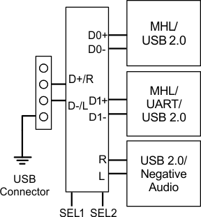
The TS3USBA225 is a 2-channel single-pole triple-throw (SP3T) multiplexer that supports USB 2.0 High-Speed (480 Mbps) signals in all 3 differential channels. The first two high-speed differential channels also support Mobile High Definition Link (MHL) signaling with resolution and video frame rates up to 720p, 60 fps and 1080i, 30 fps. The remaining differential channel can also be used as an audio switch that is designed to allow analog audio signals to swing negatively. This configuration allows the system designer to use a common connector for audio and USB 2.0 or MHL data.
The TS3USBA225 has a VCC range of 2.7 V to 5.0 V with the capability to pass true-ground audio signals down to –1.8 V. The device also supports a power-down mode that can be enabled when both SEL1 and SEL2 controls are low to minimize current consumption when no signal is transmitting. The TS3USBA225 also features internal shunt resistors on the audio path to reduce clicks and pops that may be heard when the audio switches are selected.
Device Information(1)
| PART NUMBER | PACKAGE | BODY SIZE (NOM) |
|---|---|---|
| TS3USBA225 | UQFN (12) | 2.00 mm × 1.70 mm |
- For all available packages, see the orderable addendum at the end of the data sheet.
4 Revision History
Changes from B Revision (July 2012) to C Revision
- Added Device Information table, ESD Ratings table, Thermal Information table, Detailed Description section, Application and Implementation section, Power Supply Recommendations section, Layout section, Device and Documentation Support section, and Mechanical, Packaging, and Orderable Information sectionGo
- Correct typographical errors to align datasheet information. Go
- Changed "Negative Rail Capability -1.8 V to VCC" to “Negative Rail Capability down to -1.8 V” in Features. Go
- Updated Recommended Operating Conditions table. Go
- Updated Typical Characteristics graphs. Go
Changes from A Revision (April 2012) to B Revision
- Updated Application Block Diagrams.Go
- Updated MIN value in the Absolute Maximum Ratings table for VR, VL.Go
- Updated MIN value in the Recommended Operating Conditions table for VR, VL.Go
Changes from * Revision (October 2011) to A Revision
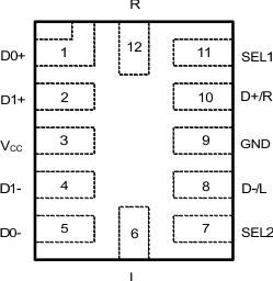
5 Pin Configuration and Functions

Pin Functions
| PIN | I/O | DESCRIPTION | |
|---|---|---|---|
| NAME | NO. | ||
| D0+ | 1 | I/O | MHL/USB/UART Data 1 (Differential +) |
| D1+ | 2 | I/O | MHL/USB/UART Data 2 (Differential +) |
| VCC | 3 | - | Power supply |
| D1– | 4 | I/O | MHL/USB/UART Data 2 (Differential –) |
| D0– | 5 | I/O | MHL/USB/UART Data 1 (Differential –) |
| L | 6 | I/O | USB-/Left Channel Audio |
| SEL2 | 7 | I | Control Input Select Line 2. The default state for SEL2 is LOW. |
| D–/L | 8 | I/O | MHL/USB/UART/Audio Common Connector |
| GND | 9 | - | Ground |
| D+/R | 10 | I/O | MHL/USB/UART/Audio Common Connector |
| SEL1 | 11 | I | Control Input Select Line 1. The default state for SEL1 is LOW. |
| R | 12 | I/O | USB+/Right Channel Audio |
6 Specifications
6.1 Absolute Maximum Ratings(1)(2)(3)
over operating free-air temperature range (unless otherwise noted)| MIN | MAX | UNIT | |||
|---|---|---|---|---|---|
| VCC | Supply voltage | –0.3 | 6.0 | V | |
| VD0+, VD0-, VD1+, VD1- |
High speed differential signal voltage | –0.3 | 4.6 | V | |
| VR, VL | Audio signal voltage | – 1.9 | 4.6 | V | |
| IK | Analog port diode current | VI/O+ ,VI/O- < 0 | –50 | mA | |
| VI | Digital input voltage (SEL1, SEL2) | –0.3 | 6.0 | V | |
| IIK | Digital logic input clamp current(3) | VI < 0 | –50 | ||
| ICC | Continuous current through VCC | 100 | mA | ||
| IGND | Continuous current through GND | –100 | mA | ||
| Tstg | Storage temperature | –65 | 150 | °C | |
6.2 ESD Ratings
| VALUE | UNIT | |||
|---|---|---|---|---|
| V(ESD) | Electrostatic discharge | Human-body model (HBM), per ANSI/ESDA/JEDEC JS-001(1) | ±2000 | V |
| Charged-device model (CDM), per JEDEC specification JESD22-C101(2) | ±1000 | |||
6.3 Recommended Operating Conditions
| MIN | MAX | UNIT | |||
|---|---|---|---|---|---|
| VCC | Supply voltage range | 2.7 | 5.0 | V | |
| VD0+, VD0-, VD1+, VD1- |
High speed differential signal voltage range | 0 | 4.5 | V | |
| VR, VL | Audio signal voltage range when not in power-down mode | –1.8 | 4.3 V or VCC(1) | V | |
| Audio signal voltage range when in power-down mode | –1 | 1 | |||
| IK | Analog port diode current | VI/O+ ,VI/O- < 0 | –50 | mA | |
| VI | Digital input voltage range (SEL1, SEL2) | 0 | VCC | V | |
| TA | Operating free-air temperature | –40 | 85 | °C | |
6.4 Thermal Information
| THERMAL METRIC (1) | TS3USBA225 | UNIT | |
|---|---|---|---|
| RUT (UQFN) | |||
| 12 PINS | |||
| RθJA | Junction-to-ambient thermal resistance | 118.6 | °C/W |
| RθJC(top) | Junction-to-case (top) thermal resistance | 45.1 | °C/W |
| RθJB | Junction-to-board thermal resistance | 47.9 | °C/W |
| ψJT | Junction-to-top characterization parameter | 0.7 | °C/W |
| ψJB | Junction-to-board characterization parameter | 47.9 | °C/W |
6.5 Electrical Characteristics
TA = –40°C to 85°C, typical values are at VCC = 3.3 V, TA = 25°C (unless otherwise noted)| PARAMETER | TEST CONDITIONS | MIN | TYP | MAX | UNIT | ||
|---|---|---|---|---|---|---|---|
| MHL/USB SWITCH | |||||||
| ron | ON-state resistance | VCC = 3.0 V | VI/O+,I/O- = 0.4 V, ION = 15 mA | 6.5 | 7.5 | Ω | |
| Δron | ON-state resistance match between channels | VCC = 3.0 V | VI/O+,I/O- = 1.7 V, ION = 15 mA | 0.1 | Ω | ||
| ron (flat) | ON-state resistance flatness | VCC = 3.0 V | VI/O+,I/O- = 0 to 1.7 V, ION = 15 mA | 0.5 | Ω | ||
| IOZ | OFF leakage current | VCC = 3.6 V | Switch OFF , VI/O+,I/O- = 0 to 3.6 V, VD+/R, D-/L = 0 V |
1 | µA | ||
| USB/AUDIO SWITCH | |||||||
| ron | ON-state resistance | VCC = 3.0 V | SEL1 = High, SEL2 = Low, VL/R = –1.8 V, 0 V, 0.7 V, ION = –26 mA |
2.5 | 3.5 | Ω | |
| Δron | ON-state resistance match between channels | VCC = 3.0 V | SEL1 = High, SEL2 = Low, VL/R = 0.7 V, ION = –26 mA |
0.1 | Ω | ||
| ron (flat) | ON-state resistance flatness | VCC = 3.0 V | SEL1 = High, SEL2 = Low, VL/R = –1.8 V, 0 V, 0.7 V, ION = –26 mA |
0.1 | Ω | ||
| rSHUNT | Shunt resistance | VCC = 2.7 V to 5.0 V | Switch OFF, VL/R = 0.7 V, ISHUNT = 10 mA |
100 | 200 | Ω | |
| DIGITAL CONTROL INPUTS (SEL1, SEL2) | |||||||
| VIH | Input logic high | VCC = 3.3 V to 5.0 V | 1.3 | V | |||
| VIL | Input logic low | VCC = 2.7 V to 3.3 V | 0.25 | V | |||
| VCC = 3.3 V to 5.0 V | 0.4 | ||||||
| IIN | Input leakage current | VCC = 2.7 V to 5.0 V | VIN = 5.0 V | ±3 | μA | ||
| VIN = 0 V | ±0.1 | ||||||
| rPD1, rPD2 | Internal pulldown resistance | VCC = 2.7 V to 5.0 V | 3 | MΩ | |||
6.6 Dynamic Characteristics
TA = –40°C to 85°C, typical values are at VCC = 3.3 V, TA = 25°C (unless otherwise noted)| PARAMETER | TEST CONDITIONS | MIN | TYP | MAX | UNIT | ||
|---|---|---|---|---|---|---|---|
| MHL/USB SWITCH | |||||||
| tpd | Propagation Delay | VCC = 2.7 V or 3.3 V | 0.25 | ns | |||
| tON | Turn-on time | RL = 50 Ω, CL = 35 pF | VCC = 2.7 V | 60 | ns | ||
| tOFF | Turn-off time | RL = 50 Ω, CL = 35 pF | VCC = 2.7 V | 20 | ns | ||
| tSK(O) | Channel-to-channel skew | VCC = 2.7 V or 3.3 V | 15 | ps | |||
| tSK(P) | Skew of opposite transitions of same output | VCC = 2.7 V or 3.3 V | 15 | ps | |||
| CI/O+(OFF)
CI/O-(OFF) |
OFF capacitance | VCC = 2.7 V or 3.3 V, VD0+/D0- =0 or 3.3 V |
Switch OFF | 1 | pF | ||
| CI/O+(ON)
CI/O-(ON) |
ON capacitance | VCC = 2.7 V or 3.3 V, VD0+/D0- = 0 or 3.3 V |
Switch ON | 3 | pF | ||
| CI | Digital input capacitance | VCC = 2.7 V or 3.3 V, VI = 0 or 3.3 V | 2.5 | pF | |||
| BW | Bandwidth | VCC = 2.7 V or 3.3 V, RL = 50 Ω | Switch ON | 1.9 | GHz | ||
| OISO | OFF Isolation | VCC = 2.7 V or 3.3 V, RL = 50 Ω, f = 240 MHz |
Switch OFF | -35 | dB | ||
| XTALK | Crosstalk | VCC = 2.5 V or 3.3 V, RL = 50 Ω, f = 240 MHz |
Switch ON | -45 | dB | ||
| USB/AUDIO SWITCH | |||||||
| tON | Turn-on time | RL = 50 Ω, CL = 35 pF | VCC = 2.7 V | 40 | µs | ||
| tOFF | Turn-off time | RL = 50 Ω, CL = 35 pF | VCC = 2.7 V | 15 | ns | ||
| CL(OFF), CR(OFF) | L , R OFF capacitance | VCC = 2.7 V to 4.5 V, f = 20 kHz | Switch OFF | 1.0 | pF | ||
| CL(ON), CR(ON) | L, R ON capacitance | VCC = 2.7 V to 4.5 V, f = 20 kHz | Switch ON | 3.5 | pF | ||
| OISO | OFF Isolation | VCC = 3.3 V, RL = 50 Ω, f = 20 kHz | Switch OFF | -85 | dB | ||
| XTALK | Crosstalk | VCC = 3.3 V, RL = 50 Ω, f = 20 kHz | Switch ON | -95 | dB | ||
| THD | Total harmonic distortion | VCC = 3.3 V, SEL1 = High, SEL2 = Low, f = 20 Hz to 20 kHz, RL = 600 Ω, VIN = 2 Vpp |
Switch ON | 0.05% | |||
| SUPPLY | |||||||
| VCC | Power supply voltage | 2.7 | 5.0 | V | |||
| ICC | Positive supply current | VCC = 2.7 V, 3.6 V, 5.0 V VIN= VCC or GND, VI/O = 0 V, Switch ON or OFF |
25 | 50 | µA | ||
| ICC, PD | Positive supply current (Power-Down Mode) | VCC = 2.7 V, 3.6 V, 5.0 V, VI/O = 0 V, SEL1 and SEL2 = Low |
3 | 5 | µA | ||
| PSRR | Power Supply Rejection Ratio | VCC = 2.7 V, 3.6 V, 5.0 V VIN = VCC +/- 200 mVpp RL = 50 Ω |
-60 | dB | |||
| IOFF | Power off leakage current | VCC = 0 V, D+/R, D-/L, D0+, D0-, D1+, D1-, L, VIN = 0 to 4.5 V |
±0.1 | µA | |||
6.7 Typical Characteristics


7 Detailed Description
7.1 Overview
The TS3USBA225 is a 2-channel single-pole triple-throw (SP3T) multiplexer that supports USB 2.0 High-Speed (480 Mbps) signals in all 3 differential channels. The first two high-speed differential channels also support Mobile High Definition Link (MHL) signaling with video resolution and frame rates up to 720p, 60 fps and 1080i, 30 fps. The remaining differential channel can also be used as an audio switch that is designed to allow analog audio signals to swing negatively. This configuration allows the system designer to use a common connector for audio and USB 2.0 or MHL data.
The TS3USBA225 has a VCC range of 2.7 V to 5.0 V with the capability to pass true-ground audio signals down to –1.8 V. The device also supports a power-down mode that can be enabled when both SEL controls are low to minimize current consumption when no signal is transmitting. The TS3USBA225 also features internal shunt resistors on the audio path to reduce clicks and pops that may be heard when the audio switches are selected.
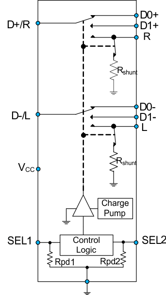
7.2 Functional Block Diagram

7.3 Feature Description
7.3.1 Click and Pop Reduction
The shunt resistors in the TS3USBA225 automatically discharge any capacitance at the L and R terminals when they are not connected to the common D-/L and D+/R paths. This reduces the audible click-and-pop sounds that occur when switching between audio sources. Audible clicks and pops are caused when a step DC voltage is switched into the speaker. By automatically discharging the side that is not connected, any residual DC voltage is removed, thereby reducing the clicks and pops.
7.3.2 Negative Signal Swing Capability
The TS3USBA225 has an analog audio path L and R that can support negative signals that pass below ground without distortion. These analog switches operate from –1.8 V to 4.3 V.
7.4 Device Functional Modes
7.4.1 High Impedance (Hi-Z) Mode
The TS3USBA225 has a Hi-Z mode that places the device's signal paths in a high impedance state when there is no power supplied to the TS3USBA225 VCC pin. This mode will isolate the signal bus in a powered off situation so that it may not interfere with other devices that maybe sharing the bus.
7.4.1.1 Power-Down Mode
The TS3USBA225 has a power-down mode that reduces the power consumption to 3 μA when the device is not in use. To put the device in power-down mode and disable the switch, the SEL1 and SEL2 pins must be supplied with a logic low signal.
7.4.2 Device Functional Modes
Table 1 is the function table for the TS3USBA225.

