SLUSAG0A March 2011 – March 2016 UC1707-SP
PRODUCTION DATA.
- 1 Features
- 2 Applications
- 3 Description
- 4 Revision History
- 5 Pin Configuration and Functions
- 6 Specifications
- 7 Parameter Measurement Information
- 8 Detailed Description
- 9 Application and Implementation
- 10Power Supply Recommendations
- 11Layout
- 12Device and Documentation Support
- 13Mechanical, Packaging, and Orderable Information
Package Options
Mechanical Data (Package|Pins)
Thermal pad, mechanical data (Package|Pins)
Orderable Information
1 Features
- Rad-Tolerant: 50 kRad (Si) for 5962-8761903VEA, 5962-8761903VFA (1)
- QML-V Qualified, SMD
(5962-8761901VEA, 5962-8761903VEA,
5962-8761903VFA, 5962-8761901V2A) - Two Independent Drivers
- 1.5-A Totem Pole Outputs
- Inverting and Non-Inverting Inputs
- 40-ns Rise and Fall Into 1000 pF
- High-Speed, Power MOSFET Compatible
- Low Cross-Conduction Current Spike
- Analog Shutdown With Optional Latch
- Low Quiescent Current
- 5-V to 40-V Operation
- Thermal Shutdown Protection
- 16-Pin Dual-In-Line Package
2 Applications
- Switch Mode Power Supply
- DC-DC Converter
- Pulse Transformer Driver

3 Description
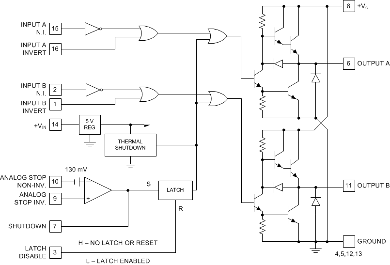
The UC1707-SP power driver is made with a high-speed Schottky process to interface between low-level control functions and high-power switching devices – particularly power MOSFETs. The UC1707-SP contains two independent channels, each of which can be activated by either a high or low input logic level signal. Each output can source or sink up to 1.5 A as long as power dissipation limits are not exceeded.
Although each output can be activated independently with its own inputs, it can be forced low in common through the action either of a digital high signal at the Shutdown terminal or a differential low-level analog signal. The Shutdown command from either source can either be latching or not, depending on the status of the Latch Disable pin.
Supply voltage for both VIN and VC can independently range from 5 to 40 V.
Device Information(1)
| PART NUMBER | PACKAGE | BODY SIZE (NOM) |
|---|---|---|
| UC1707-SP | CDIP (16) | 6.92 mm × 19.56 mm |
| CFP (16) | 6.73 mm × 10.30 mm | |
| LCCC (20) | 8.89 mm × 8.89 mm |
- For all available packages, see the orderable addendum at the end of the data sheet.
Truth Table
(Each Channel)(1)
| INV. | N.I. | OUT |
|---|---|---|
| H | H | L |
| L | H | H |
| H | L | L |
| L | L | L |
OUT = INV or N.I.
4 Revision History
Changes from * Revision (March 2011) to A Revision
- Added ESD Ratings table, Recommended Operating Conditions table, Thermal Information table, Feature Description section, Device Functional Modes, Application and Implementation section, Power Supply Recommendations section, Layout section, Device and Documentation Support section, and Mechanical, Packaging, and Orderable Information section Go
- Corrected typos in Pin Configuration and FunctionsGo
- Deleted package thermal impedance in Absolute Maximum Ratings tableGo
- Added Community Resources Go