SLUS352C January 1997 – December 2015 UC1846 , UC2846 , UC3846 , UC3847
PRODUCTION DATA.
- 1 Features
- 2 Applications
- 3 Description
- 4 Revision History
- 5 Pin Configuration and Functions
- 6 Specifications
- 7 Detailed Description
- 8 Application and Implementation
- 9 Power Supply Recommendations
- 10Layout
- 11Device and Documentation Support
- 12Mechanical, Packaging, and Orderable Information
Package Options
Refer to the PDF data sheet for device specific package drawings
Mechanical Data (Package|Pins)
- J|16
Thermal pad, mechanical data (Package|Pins)
Orderable Information
1 Features
- Automatic Feedforward Compensation
- Programmable Pulse-by-Pulse Current Limiting
- Automatic Symmetry Correction in Push-Pull Configuration
- Enhanced Load Response Characteristics
- Parallel Operation Capability for Modular Power Systems
- Differential Current Sense Amplifier with Wide Common Mode Range
- Double-Pulse Suppression
- 500-mA (Peak) Totem-pole Outputs
- ±1% Band Gap Reference
- Undervoltage Lockout
- Soft-Start Capability
- Shutdown Terminal
- 500-kHz Operation
2 Applications
- Telecommunication Power Converters
- Industrial Power Converters
3 Description
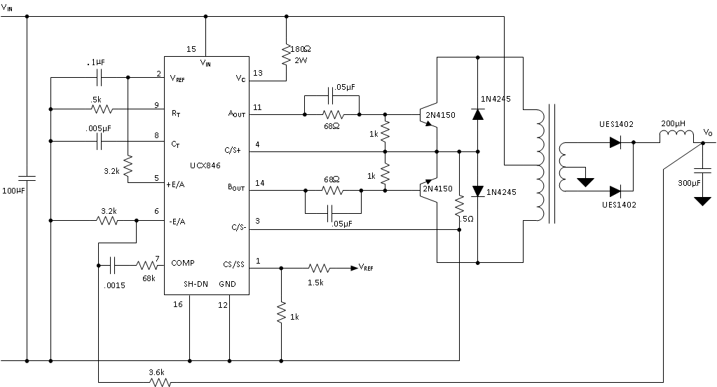
The UC1846/7 family of control devices provides all of the necessary features to implement fixed-frequency, current-mode control schemes while maintaining a minimum external parts count. The superior performance of this technique can be measured in improved line regulation, enhanced load response characteristics, and a simpler, easier-to-design control loop. Topological advantages include inherent pulse-by-pulse current limiting capability, automatic symmetry correction for push-pull converters, and the ability to parallel power modules while maintaining equal current sharing.
Protection circuitry includes built-in undervoltage lockout and programmable current limit, in addition to soft-start capability. A shutdown function is also available, which can initiate either a complete shutdown with automatic restart or latch the supply off.
Other features include fully-latched operation, double-pulse suppression, deadline adjust capability, and a ±1% trimmed band gap reference.
The UC1846 features low outputs in the OFF state, while the UCx847 features high outputs in the OFF state.
Device Information(1)
| PART NUMBER | PACKAGE | BODY SIZE (NOM) |
|---|---|---|
| UC1846 | LCCC (20) | 8.89 mm × 8.89 mm |
| CDIP (16) | 6.92 mm × 19.56 mm | |
| UC2846, UC3846 | PLCC (20) | 8.96 mm × 8.96 mm |
| SOIC (16) | 7.5 mm × 10.3 mm | |
| PDIP (16) | 6.35 mm × 19.3 mm | |
| UC2847, UC3847 | SOIC (16) | 7.5 mm × 10.3 mm |
| PDIP (16) | 6.35 mm × 19.3 mm |
- For all available packages, see the orderable addendum at the end of the datasheet.
