-
UCC21710-Q1 10A Source/Sink Reinforced Isolated Single Channel Gate Driver for SiC/IGBT with Active Protection, Isolated Analog Sensing and High-CMTI
- 1
- 1 Features
- 2 Applications
- 3 Description
- 4 Pin Configuration and Functions
-
5 Specifications
- 5.1 Absolute Maximum Ratings
- 5.2 ESD Ratings
- 5.3 Recommended Operating Conditions
- 5.4 Thermal Information
- 5.5 Power Ratings
- 5.6 Insulation Specifications
- 5.7 Safety-Related Certifications
- 5.8 Safety Limiting Values
- 5.9 Electrical Characteristics
- 5.10 Switching Characteristics
- 5.11 Insulation Characteristics Curves
- 5.12 Typical Characteristics
- 6 Parameter Measurement Information
-
7 Detailed Description
- 7.1 Overview
- 7.2 Functional Block Diagram
- 7.3
Feature Description
- 7.3.1 Power Supply
- 7.3.2 Driver Stage
- 7.3.3 VCC and VDD Undervoltage Lockout (UVLO)
- 7.3.4 Active Pulldown
- 7.3.5 Short Circuit Clamping
- 7.3.6 Internal Active Miller Clamp
- 7.3.7 Overcurrent and Short Circuit Protection
- 7.3.8 Soft Turn-off
- 7.3.9 Fault ( FLT, Reset and Enable ( RST/EN)
- 7.3.10 Isolated Analog to PWM Signal Function
- 7.4 Device Functional Modes
-
8 Applications and Implementation
- 8.1 Application Information
- 8.2
Typical Application
- 8.2.1 Design Requirements
- 8.2.2
Detailed Design Procedure
- 8.2.2.1 Input filters for IN+, IN- and RST/EN
- 8.2.2.2 PWM Interlock of IN+ and IN-
- 8.2.2.3 FLT, RDY and RST/EN Pin Circuitry
- 8.2.2.4 RST/EN Pin Control
- 8.2.2.5 Turn on and turn off gate resistors
- 8.2.2.6 Overcurrent and Short Circuit Protection
- 8.2.2.7 Isolated Analog Signal Sensing
- 8.2.2.8 Higher Output Current Using an External Current Buffer
- 9 Power Supply Recommendations
- 10Layout
- 11Device and Documentation Support
- 12Revision History
- 13Mechanical, Packaging, and Orderable Information
- IMPORTANT NOTICE
Package Options
Mechanical Data (Package|Pins)
- DW|16
Thermal pad, mechanical data (Package|Pins)
- DW|16
Orderable Information
UCC21710-Q1 10A
Source/Sink Reinforced Isolated Single Channel Gate Driver
for SiC/IGBT with Active Protection, Isolated Analog Sensing and High-CMTI
1 Features
- 5.7kVRMS single channel isolated gate driver
- AEC-Q100 qualified for automotive applications
- Device temperature grade 1: -40°C to +125°C ambient operating temperature range
- SiC MOSFETs and IGBTs up to 2121Vpk
- 33V maximum output drive voltage (VDD-VEE)
- ±10A drive strength and split output
- 150V/ns minimum CMTI
- 270ns response time fast overcurrent protection
- 4A internal active miller clamp
- 400mA soft turn-off when fault happens
- Isolated analog sensor with PWM
output for
- Temperature sensing with NTC, PTC or thermal diode
- High voltage DC-Link or phase voltage
- Alarm FLT on over current and reset from RST/EN
- Fast enable/disable response on RST/EN
- Reject <40ns noise transient and pulse on input pins
- 12V VDD UVLO with power good on RDY
- Inputs/outputs with over/under-shoot transient voltage Immunity up to 5V
- 130ns (maximum) propagation delay and 30ns (maximum) pulse/part skew
- SOIC-16 DW package with creepage and clearance distance > 8mm
- Operating junction temperature –40°C to 150°C
- Safety-related certifications:
- Reinforced insulation per DIN EN IEC 60747-17(VDE 0884-17)
- UL 1577 component recognition program
2 Applications
- Traction inverter for EVs
- On-board charger and charging pile
- DC/DC Converter for HEV/EVs
3 Description
The UCC21710-Q1 is a galvanic isolated single channel gate driver designed for up to 1700-V SiC MOSFETs and IGBTs with advanced protection features, best-in-class dynamic performance and robustness. UCC21710-Q1 has up to ±10A peak source and sink current.
The input side is isolated from the output side with SiO2 capacitive isolation technology, supporting up to 1.5kVRMS working voltage, 12.8kVPK surge immunity with longer than 40 years Isolation barrier life, as well as providing low part-to-part skew , and >150V/ns common mode noise immunity (CMTI).
The UCC21710-Q1 includes the state-of-the-art protection features, such as fast overcurrent and short circuit detection, shunt current sensing support, fault reporting, active Miller clamp, and input and output side power supply UVLO to optimize SiC and IGBT switching behavior and robustness. The isolated analog to PWM sensor can be used for easier temperature or voltage sensing, further increasing the drivers' versatility and simplifying the system design effort, size and cost.
| PART NUMBER | PACKAGE(1) | BODY SIZE (NOM) |
|---|---|---|
| UCC21710-Q1 | DW (SOIC-16) | 10.3mm × 7.5mm |
 Device Pin Configuration
4 Pin Configuration and Functions
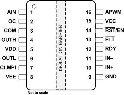 Figure 4-1 UCC21710-Q1DW SOIC (16)Top View
| PIN | I/O(1) | DESCRIPTION | |
|---|---|---|---|
| NAME | NO. | ||
| AIN | 1 | I | Isolated analog sensing input, parallel a small capacitor to COM for better noise immunity. Tie to COM if unused. |
| OC | 2 | I | Over current detection pin, support lower threshold for SenseFET, DESAT, and shunt resistor sensing. Tie to COM if unused. |
| COM | 3 | P | Common ground reference, connecting to emitter pin for IGBT and source pin for SiC-MOSFET |
| OUTH | 4 | O | Gate driver output pull up |
| VDD | 5 | P | Positive supply rail for gate drive voltage. Bypass with a >10-μF capacitor to COM to support specified gate driver source peak current capability. Place decoupling capacitor close to the pin. |
| OUTL | 6 | O | Gate driver output pull down |
| CLMPI | 7 | I | Internal Active miller clamp, connecting this pin directly to the gate of the power transistor. Leave floating or tie to VEE if unused. |
| VEE | 8 | P | Negative supply rail for gate drive voltage. Bypass with a >10-μF capacitor to COM to support specified gate driver sink peak current capability. Place decoupling capacitor close to the pin. |
| GND | 9 | P | Input power supply and logic ground reference |
| IN+ | 10 | I | Non-inverting gate driver control input. Tie to VCC if unused. |
| IN– | 11 | I | Inverting gate driver control input. Tie to GND if unused. |
| RDY | 12 | O | Power good for VCC-GND and VDD-COM. RDY is open drain configuration and can be paralleled with other RDY signals |
| FLT | 13 | O | Active low fault alarm output upon over current or short circuit. FLT is in open drain configuration and can be paralleled with other faults |
| RST/EN | 14 | I | The RST/EN serves two purposes: 1) Enable / shutdown of the output side. The FET is turned off by a regular turn-off, if terminal EN is set to low; 2) Resets the DESAT condition signaled on FLT pin. if terminal RST/EN is set to low for more than 1000ns. A reset of signal FLT is asserted at the rising edge of terminal RST/EN. For automatic RESET function, this pin only serves as an EN pin. Enable / shutdown of the output side. The FET is turned off by a general turn-off, if terminal EN is set to low. |
| VCC | 15 | P | Input power supply from 3V to 5.5V. Bypass with a >1-μF capacitor to GND. Place decoupling capacitor close to the pin. |
| APWM | 16 | O | Isolated Analog Sensing PWM output. Leave floating if unused. |
5 Specifications
5.1 Absolute Maximum Ratings
| PARAMETER | MIN | MAX | UNIT | ||
|---|---|---|---|---|---|
| VCC | VCC – GND | –0.3 | 6 | V | |
| VDD | VDD – COM | –0.3 | 36 | V | |
| VEE | VEE – COM | –17.5 | 0.3 | V | |
| VMAX | VDD – VEE | –0.3 | 36 | V | |
| IN+, IN–, RST/EN | DC | GND–0.3 | VCC | V | |
| Transient, less than 100 ns(2) | GND–5.0 | VCC+5.0 | V | ||
| AIN | Reference to COM | –0.3 | 5 | V | |
| OC | Reference to COM | -0.3 | 6 | ||
| OUTH, OUTL , CLMPI | DC | VEE–0.3 | VDD | V | |
| Transient, less than 100 ns(2) | VEE–5.0 | VDD+5.0 | V | ||
| RDY, FLT, APWM | GND–0.3 | VCC | V | ||
| IFLT, IRDY | FLT, and RDY pin input current | 20 | mA | ||
| IAPWM | APWM pin output current | 20 | mA | ||
| TJ | Junction temperature range | –40 | 150 | °C | |
| Tstg | Storage temperature range | –65 | 150 | °C | |
5.2 ESD Ratings
| VALUE | UNIT | |||
|---|---|---|---|---|
| V(ESD) | Electrostatic discharge | Human-body model (HBM), per AEC Q100-002(1) | ±4000 | V |
| Charged-device model (CDM), per AEC Q100-011 | ±1500 | |||
5.3 Recommended Operating Conditions
| PARAMETER | MIN | MAX | UNIT | ||
|---|---|---|---|---|---|
| VCC | VCC–GND | 3.0 | 5.5 | V | |
| VDD | VDD–COM | 13 | 33 | V | |
| VMAX | VDD–VEE | – | 33 | V | |
| IN+, IN–, RST/EN | Reference to GND | High level input voltage | 0.7×VCC | VCC | V |
| Low level input voltage | 0 | 0.3×VCC | |||
| AIN | Reference to COM | 0.6 | 4.5 | V | |
| tRST/EN | Minimum pulse width that reset the fault | 1000 | ns | ||
| TA | Ambient Temperature | –40 | 125 | °C | |
| TJ | Junction temperature | –40 | 150 | °C | |
5.4 Thermal Information
| THERMAL METRIC(1) | UCC21710-Q1 | UNIT | |
|---|---|---|---|
| DW (SOIC) | |||
| 16-PINS | |||
| RθJA | Junction-to-ambient thermal resistance | 68.3 | °C/W |
| RθJC(top) | Junction-to-case (top) thermal resistance | 27.5 | °C/W |
| RθJB | Junction-to-board thermal resistance | 32.9 | °C/W |
| ψJT | Junction-to-top characterization parameter | 14.1 | °C/W |
| ψJB | Junction-to-board characterization parameter | 32.3 | °C/W |
5.5 Power Ratings
| PARAMETER | TEST CONDITIONS | Value | UNIT | |
|---|---|---|---|---|
| PD | Maximum power dissipation (both sides) | VCC = 5V, VDD-COM = 20V, COM-VEE = 5V, IN+/- = 5V, 150kHz, 50% Duty Cycle for 10nF load, Ta=25oC | 985 | mW |
| PD1 | Maximum power dissipation by transmitter side | 20 | mW | |
| PD2 | Maximum power dissipation by receiver side | 965 | mW | |
5.6 Insulation Specifications
| PARAMETER | TEST CONDITIONS | VALUE | UNIT | |
|---|---|---|---|---|
| GENERAL | ||||
| CLR | External clearance(1) | Shortest terminal-to-terminal distance through air | > 8 | mm |
| CPG | External creepage(1) | Shortest terminal-to-terminal distance across the package surface | > 8 | mm |
| DTI | Distance through the insulation | Minimum internal gap (Internal clearance) of the double insulation (2 × 0.0085 mm) | > 17 | µm |
| CTI | Comparative tracking index | DIN EN 60112 (VDE 0303-11); IEC 60112 | > 600 | V |
| Material group | According to IEC 60664–1 | I | ||
| Overvoltage Category per IEC 60664–1 | Rated mains voltage ≤ 300 VRMS | I-IV | ||
| Rated mains voltage ≤ 600 VRMS | I-IV | |||
| Rated mains voltage ≤ 1000 VRMS | I-III | |||
| DIN EN IEC 60747-17 (VDE 0884-17)(2) | ||||
| VIORM | Maximum repetitive peak isolation voltage | AC voltage (bipolar) | 2121 | VPK |
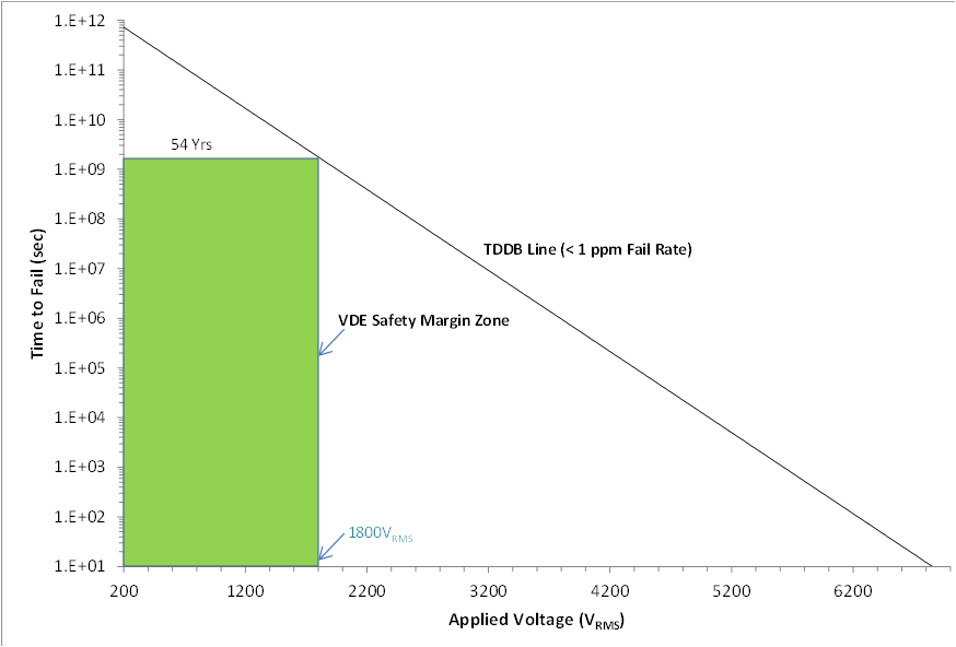
| VIOWM | Maximum isolation working voltage | AC voltage (sine wave) Time dependent dielectric breakdown (TDDB) test | 1500 | VRMS |
| DC voltage | 2121 | VDC | ||
| VIMP | Maximum impulse voltage | Tested in air, 1.2/50-μs waveform per IEC 62368-1 | 8000 | VPK |
| VIOTM | Maximum transient isolation voltage | VTEST=VIOTM, t = 60 s (qualification test) | 8000 | VPK |
| VTEST=1.2 x VIOTM, t = 1 s (100% production test) | ||||
| VIOSM | Maximum surge isolation voltage(3) | Test method per IEC 62368-1, 1.2/50 µs waveform, VTEST = 1.6 × VIOSM = 12800 VPK (qualification) | 8000 | VPK |
| qpd | Apparent charge(4) | Method a: After I/O safety test subgroup 2/3, Vini = VIOTM, tini = 60 s; Vpd(m) = 1.2 × VIORM = 2545 VPK, tm = 10 s | ≤ 5 | pC |
| Method a: After environmental tests subgroup 1, Vini = VIOTM, tini = 60 s; Vpd(m) = 1.6 × VIORM = 3394 VPK, tm = 10 s | ≤ 5 | |||
| Method b1: At routine test (100% production) and preconditioning (type test) Vini = VIOTM, tini = 1 s; Vpd(m) = 1.875 × VIORM = 3977 VPK, tm = 1 s | ≤ 5 | |||
| CIO | Barrier capacitance, input to output(5) | VIO = 0.5 sin (2πft), f = 1 MHz | ~ 1 | pF |
| RIO | Insulation resistance, input to output(5) | VIO = 500 V, TA = 25°C | ≥ 1012 | Ω |
| VIO = 500 V, 100°C ≤ TA ≤ 125°C | ≥ 1011 | |||
| VIO = 500 V at TS = 150°C | ≥ 109 | |||
| Pollution degree | 2 | |||
| Climatic category | 40/125/21 | |||
| UL 1577 | ||||
| VISO | Withstand isolation voltage | VTEST = VISO = 5700 VRMS, t = 60 s (qualification); VTEST = 1.2 × VISO = 6840 VRMS, t = 1 s (100% production) | 5700 | VRMS |
5.7 Safety-Related Certifications
| VDE | UL |
|---|---|
| Certified according to DIN EN IEC 60747-17 (VDE 0884-17) | Recognized under UL 1577 Component Recognition Program, CSA Component Acceptance Notice 5A |
| Reinforced insulation Maximum transient isolation voltage, 8000 VPK; Maximum repetitive peak isolation voltage, 2121 VPK; Maximum surge isolation voltage, 8000 VPK |
Single protection, 5700 VRMS |
| Certificate number: 40040142 | File Number: E181974 |
5.8 Safety Limiting Values
| PARAMETER | TEST CONDITIONS | MIN | TYP | MAX | UNIT | |
|---|---|---|---|---|---|---|
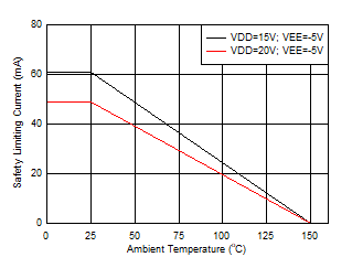
| IS | Safety input, output, or supply current | RθJA =68.3°C/W, VDD = 15V, VEE=-5V, TJ = 150°C, TA = 25°C | 61 | mA | ||
| RθJA =68.3°C/W, VDD = 20V, VEE=-5V, TJ = 150°C, TA = 25°C | 49 | |||||
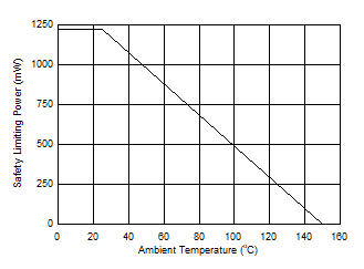
| PS | Safety input, output, or total power | RθJA =68.3°C/W, VDD = 20V, VEE=-5V, TJ = 150°C, TA = 25°C | 1220 | mW | ||
| TS | Safety temperature | 150 | °C | |||
5.9 Electrical Characteristics
| PARAMETER | TEST CONDITIONS | MIN | TYP | MAX | UNIT | ||
|---|---|---|---|---|---|---|---|
| VCC UVLO THRESHOLD AND DELAY | |||||||
| VVCC_ON | VCC–GND | 2.55 | 2.7 | 2.85 | V | ||
| VVCC_OFF | 2.35 | 2.5 | 2.65 | ||||
| VVCC_HYS | 0.2 | ||||||
| tVCCFIL | VCC UVLO Deglitch time | 10 | µs | ||||
| tVCC+ to OUT | VCC UVLO on delay to output high | IN+ = VCC, IN– = GND | 28 | 37.8 | 50 | ||
| tVCC– to OUT | VCC UVLO off delay to output low | 5 | 10 | 15 | |||
| tVCC+ to RDY | VCC UVLO on delay to RDY high | RST/EN = VCC | 30 | 37.8 | 50 | ||
| tVCC– to RDY | VCC UVLO off delay to RDY low | 5 | 10 | 15 | |||
| VDD UVLO THRESHOLD AND DELAY | |||||||
| VVDD_ON | VDD–COM | 10.5 | 12.0 | 12.8 | V | ||
| VVDD_OFF | 9.9 | 10.7 | 11.8 | ||||
| VVDD_HYS | 0.8 | ||||||
| tVDDFIL | VDD UVLO Deglitch time | 5 | µs | ||||
| tVDD+ to OUT | VDD UVLO on delay to output high | IN+ = VCC, IN– = GND | 2 | 5 | 8 | ||
| tVDD– to OUT | VDD UVLO off delay to output low | 5 | 10 | ||||
| tVDD+ to RDY | VDD UVLO on delay to RDY high | RST/EN = FLT=High | 10 | 15 | |||
| tVDD– to RDY | VDD UVLO off delay to RDY low | 10 | 15 | ||||
| VCC, VDD QUIESCENT CURRENT | |||||||
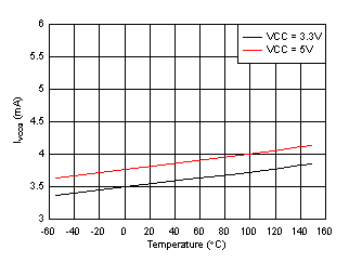
| IVCCQ | VCC quiescent current | OUT(H) = High, fS = 0Hz, AIN=2V | 2.5 | 3 | 4 | mA | |
| OUT(L) = Low, fS = 0Hz, AIN=2V | 1.45 | 2 | 2.75 | ||||
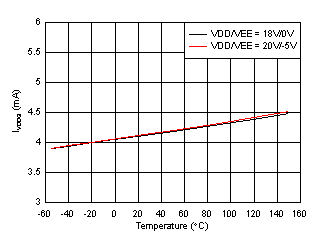
| IVDDQ | VDD quiescent current | OUT(H) = High, fS = 0Hz, AIN=2V | 3.6 | 4 | 5.9 | mA | |
| OUT(L) = Low, fS = 0Hz, AIN=2V | 3.1 | 3.7 | 5.3 | ||||
| LOGIC INPUTS — IN+, IN– and RST/EN | |||||||
| VINH | Input high threshold | VCC=3.3V | 1.85 | 2.31 | V | ||
| VINL | Input low threshold | VCC=3.3V | 0.99 | 1.52 | V | ||
| VINHYS | Input threshold hysteresis | VCC=3.3V | 0.33 | V | |||
| IIH | Input high level input leakage current | VIN = VCC | 90 | µA | |||
| IIL | Input low level input leakage | VIN = GND | –90 | µA | |||
| RIND | Input pins pull down resistance | see Detailed Description for more information | 28.5 | 55 | 113 | kΩ | |
| RINU | Input pins pull up resistance | see Detailed Description for more information | 28.5 | 55 | 113 | ||
| TINFIL | IN+, IN– and RST/EN deglitch (ON and OFF) filter time | fS = 50kHz | 28 | 40 | 60 | ns | |
| TRSTFIL | Deglitch filter time to reset /FLT | 400 | 650 | 800 | ns | ||
| GATE DRIVER STAGE | |||||||
| IOUT, IOUTH | Peak source current | CL=0.18µF, fS=1kHz | 10 | A | |||
| IOUT, IOUTL | Peak sink current | 10 | A | ||||
| ROUTH(3) | Output pull-up resistance | IOUT = –0.1A | 1.5 | 2.5 | 4.9 | Ω | |
| ROUTL | Output pull-down resistance | IOUT = 0.1A | 0.1 | 0.3 | 0.7 | Ω | |
| VOUTH | High level output voltage | IOUT = –0.2A, VDD=18V | 17.5 | V | |||
| VOUTL | Low level output voltage | IOUT = 0.2A | 60 | mV | |||
| ACTIVE PULLDOWN | |||||||
| VOUTPD | Output active pull down on OUT, OUTL | IOUTL or IOUT = 0.1×IOUT(L)(tpy), VDD=OPEN, VEE=COM | 1.5 | 2 | 2.5 | V | |
| INTERNAL ACTIVE MILLER CLAMP | |||||||
| VCLMPTH | Miller clamp threshold voltage | Reference to VEE | 1.5 | 2.0 | 2.5 | V | |
| VCLMPI | Output low clamp voltage | ICLMPI = 1A | VEE + 0.5 | V | |||
| ICLMPI | Output low clamp current | VCLMPI = 0V, VEE = –2.5V | 4 | A | |||
| RCLMPI | Miller clamp pull down resistance | ICLMPI = 0.2A | 0.6 | Ω | |||
| tDCLMPI | Miller clamp ON delay time | CL = 1.8nF | 15 | 50 | ns | ||
| SHORT CIRCUIT CLAMPING | |||||||
| VCLP-OUT(H) | VOUT–VDD, VOUTH–VDD | OUT = Low, IOUT(H) = 500mA, tCLP=10us | 0.9 | V | |||
| VCLP-OUT(L) | VOUT–VDD, VOUTL–VDD | OUT = High, IOUT(L) = 500mA, tCLP=10us | 1.8 | V | |||
| VCLP-CLMPI | VCLMPI–VDD | OUT = High, ICLMPI = 20mA, tCLP=10us | 1.0 | V | |||
| OC PROTECTION | |||||||
| IDCHG | OC pull down current when | VOC = 1V | 40 | mA | |||
| VOCTH | Detection Threshold | 0.63 | 0.7 | 0.77 | V | ||
| VOCL | Voltage when OUT(L) = LOW, Reference to COM | IOC = 5mA | 0.13 | V | |||
| tOCFIL | OC fault deglitch filter | 95 | 120 | 180 | ns | ||
| tOCOFF | OC propagation delay to OUT(L) 90% | 150 | 270 | 400 | ns | ||
| tOCFLT | OC to FLT low delay | 300 | 530 | 750 | ns | ||
| INTERNAL SOFT TURN-OFF | |||||||
| ISTO | Soft turn-off current on fault conditions | VDD-VEE=20V, VOUTL-COM=8V | 250 | 400 | 570 | mA | |
| ISOLATED TEMPERATURE SENSE AND MONITOR (AIN–APWM) | |||||||
| VAIN | Analog sensing voltage range | 0.6 | 4.5 | V | |||
| IAIN | Internal
current source |
VAIN=2.5V, -40°C< TJ< 150°C |
196 | 200 | 209 | µA | |
| fAPWM | APWM output frequency | VAIN=2.5V | 380 | 400 | 420 | kHz | |
| BWAIN | AIN–APWM bandwidth | 10 | kHz | ||||
| DAPWM | APWM Dutycycle | VAIN = 0.6V | 86.5 | 88 | 89.5 | % | |
| VAIN = 2.5V | 48.5 | 50 | 51.5 | ||||
| VAIN = 4.5V | 7.5 | 10 | 11.5 | ||||
| FLT AND RDY REPORTING | |||||||
| tRDYHLD | VDD UVLO RDY low minimum holding time | 0.55 | 1 | ms | |||
| tFLTMUTE | Output mute time on fault | Reset fault through RST/EN | 0.55 | 1 | ms | ||
| RODON | Open drain output on resistance | IODON = 5mA | 30 | Ω | |||
| VODL | Open drain low output voltage | IODON = 5mA | 0.3 | V | |||
| COMMON MODE TRANSIENT IMMUNITY | |||||||
| CMTI | Common-mode transient immunity | 150 | V/ns | ||||
5.10 Switching Characteristics
| PARAMETER | TEST CONDITIONS | MIN | TYP | MAX | UNIT | |
|---|---|---|---|---|---|---|
| tPDHL | Propagation delay time – High to Low | 60 | 90 | 130 | ns | |
| tPDLH | Propagation delay time – Low to High | 60 | 90 | 130 | ||
| PWD | Pulse width distortion |tPDHL – tPDLH| | 30 | ||||
| tsk-pp | Part to Part skew | Rising or Falling Propagation Delay | 30 | |||
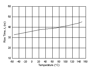
| tr | Driver output rise time | CL=10nF | 33 | |||
| tf | Driver output fall time | CL=10nF | 27 | |||
| fMAX | Maximum switching frequency | 1 | MHz | |||
5.11 Insulation Characteristics Curves
5.12 Typical Characteristics
 Figure 5-4 Output High Drive Current vs. Temperature
| IN+ = High | IN- = Low |
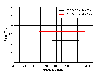 Figure 5-8 IVCCQ Supply Current vs. Input Frequency
| IN+ = Low | IN- = Low |
 Figure 5-12 VCC
UVLO vs. Temperature
| VCC = 3.3V | VDD=18V | CL = 100pF |
| RON = 0Ω | ROFF = 0Ω |
| VCC = 3.3V | VDD=18V | CL = 10nF |
| RON = 0Ω | ROFF = 0Ω |
 Figure 5-18 VOUTPD Output Active Pulldown Voltage vs.
Temperature
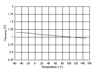
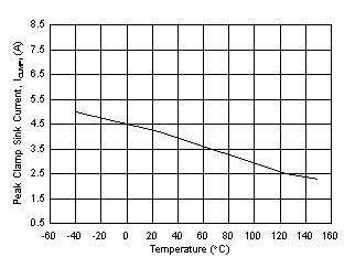
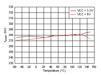
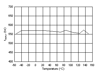
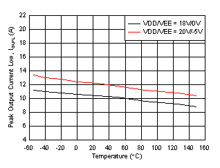 Figure 5-5 Output Low Driver Current vs. Temperature
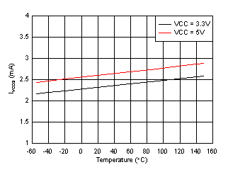
| IN+ = Low | IN- = Low |

| IN+ = High | IN- = Low |

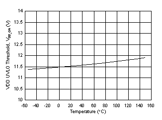 Figure 5-13 VDD
UVLO vs. Temperature
| VCC = 3.3V | VDD=18V | CL = 100pF |
| RON = 0Ω | ROFF = 0Ω |

| VCC = 3.3V | VDD=18V | CL = 10nF |
| RON = 0Ω | ROFF = 0Ω |

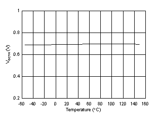
 Figure 5-21 VCLMPTH Miller Clamp Threshold Voltage vs.
Temperature
6 Parameter Measurement Information
6.1 Propagation Delay
6.1.1 Regular Turn-OFF
Figure 7-1 shows the propagation delay measurement for non-inverting configurations. Figure 7-2 shows the propagation delay measurement with the inverting configurations.
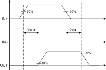 Figure 6-1 Non-inverting Logic Propagation Delay Measurement
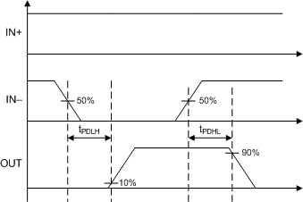 Figure 6-2 Inverting
Logic Propagation Delay Measurement
Figure 6-2 Inverting
Logic Propagation Delay Measurement6.2 Input Deglitch Filter
In order to increase the robustness of gate driver over noise transient and accidental small pulses on the input pins, i.e. IN+, IN–, RST/EN, a 40ns deglitch filter is designed to filter out the transients and make sure there is no faulty output responses or accidental driver malfunctions. When the IN+ or IN– PWM pulse is smaller than the input deglitch filter width, TINFIL, there will be no responses on OUT drive signal. Figure 6-3 and Figure 6-4 shows the IN+ pin ON and OFF pulse deglitch filter effect. Figure 6-5 and Figure 6-6 shows the IN– pin ON and OFF pulse deglitch filter effect.
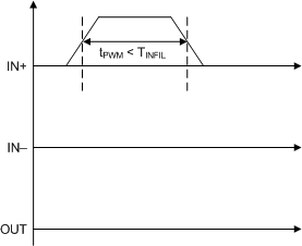 Figure 6-3 IN+ ON Deglitch Filter
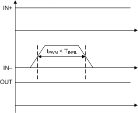 Figure 6-5 IN– ON Deglitch Filter
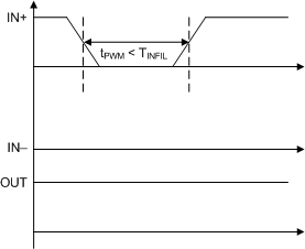 Figure 6-4 IN+ OFF Deglitch Filter
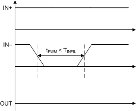 Figure 6-6 IN– OFF Deglitch Filter