UCC2870x Constant-Voltage, Constant-Current Controller With Primary-Side Regulation
1 Features
- < 30-mW No-Load Power for 5-Star Rating
- Primary-Side Regulation (PSR) Eliminates Opto-Coupler
- ±5% Voltage and Current Regulation
- 130-kHz Maximum Switching Frequency Enables High-Power Density Charger Designs
- Quasi-Resonant Valley-Switching Operation for Highest Overall Efficiency
- Patent-Pending Frequency-Jitter Scheme to Ease EMI Compliance
- Wide VDD Range Allows Small Bias Capacitor
- Clamped Gate-Drive Output for MOSFET
- Protection Functions: Overvoltage, Low-Line, and Overcurrent
- Programmable Cable Compensation (UCC28700 Only)
- NTC Resistor Interface (UCC28701, UCC28702 and UCC28703 Only) With Fixed Cable Compensation Options
- SOT-23 Package
2 Applications
- USB-Compliant Adapters and Chargers for Consumer Electronics (Cell Phones, Tablets and Cameras)
- AC and DC Power Supplies
3 Description
The UCC28700 family of flyback power supply controllers provides Constant-Voltage (CV) and Constant-Current (CC) output regulation without the use of an optical coupler. The devices process information from the primary power switch and an auxiliary flyback winding for precise control of output voltage and current. Low start-up current, dynamically controlled operating states and a tailored modulation profile support very low standby power without sacrificing start-up time or output transient response.
Control algorithms in the UCC28700 family allow operating efficiencies to meet or exceed applicable standards. The output drive interfaces to a MOSFET power switch. Discontinuous Conduction Mode (DCM) with valley switching reduces switching losses. Modulation of switching frequency and primary current peak amplitude (FM and AM) keeps the conversion efficiency high across the entire load and line ranges.
The controllers have a maximum switching frequency of 130 kHz and always maintain control of the peak-primary current in the transformer. Protection features help keep primary and secondary component stresses in check. The UCC28700 allows the level of cable compensation to be programmed. The UCC28701, UCC28702, and UCC28703 devices allow remote temperature sensing using a Negative Temperature Coefficient (NTC) resistor while providing fixed cable-compensation levels.
Device Information(1)
| PART NUMBER | PACKAGE | BODY SIZE (NOM) |
|---|---|---|
| UCC28700 | SOT-23 (6) | 2.90 mm × 1.60 mm |
| UCC28701 | ||
| UCC28702 | ||
| UCC28703 |
- For all available packages, see the orderable addendum at the end of the datasheet.
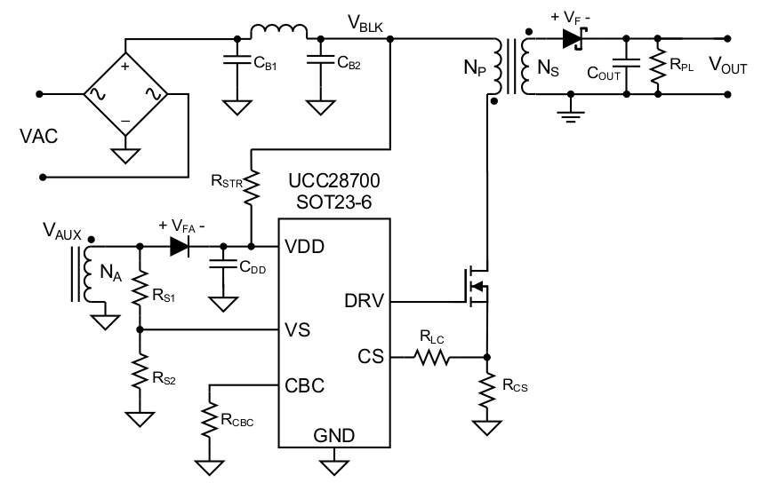
Typical Application Schematic
4 Revision History
Changes from * Revision (July 2012) to A Revision
- Added Handling Rating table, Feature Description section, Device Functional Modes, Application and Implementation section, Power Supply Recommendations section, Layout section, Device and Documentation Support section, and Mechanical, Packaging, and Orderable Information section Go
5 Device Comparison Table(1)(2)
| PART NUMBER | VERSION |
|---|---|
| UCC28700 | Programmable cable compensation |
| UCC28701 | NTC, 0 mV (at 5-V output) cable compensation option |
| UCC28702 | NTC, 150 mV (at 5-V output) cable compensation option |
| UCC28703 | NTC, 300 mV (at 5-V output) cable compensation option |
6 Pin Configuration and Functions
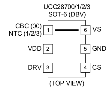
Pin Functions
| PIN | I/O | DESCRIPTION | ||
|---|---|---|---|---|
| NAME | UCC28700 | UCC28701/2/3 | ||
| NO. | NO. | |||
| CBC | 1 | — | I | Cable Compensation (CBC) is a programming pin for compensation of cable voltage drop. Cable compensation is programmed with a resistor to GND. |
| CS | 4 | 4 | I | Current Sense (CS) input connects to a ground-referenced current-sense resistor in series with the power switch. The resulting voltage is used to monitor and control the peak primary current. A series resistor can be added to this pin to compensate the peak switch current levels as the AC-mains input varies. |
| DRV | 3 | 3 | O | Drive (DRV) is an output used to drive the gate of an external high voltage MOSFET switching transistor. |
| GND | 5 | 5 | — | The Ground (GND) pin is both the reference pin for the controller and the low-side return for the drive output. Special care should be taken to return all AC decoupling capacitors as close as possible to this pin and avoid any common trace length with analog signal return paths. |
| NTC | — | 1 | I | NTC is an interface to an external NTC (negative temperature coefficient) resistor for remote temperature sensing. Pulling this pin low shuts down PWM action. |
| VDD | 2 | 2 | — | VDD is the bias supply input pin to the controller. A carefully-placed bypass capacitor to GND is required on this pin. |
| VS | 6 | 6 | I | Voltage Sense (VS) is an input used to provide voltage and timing feedback to the controller. This pin is connected to a voltage divider between an auxiliary winding and GND. The value of the upper resistor of this divider is used to program the AC-mains run and stop thresholds and line compensation at the CS pin. |
7 Specifications
7.1 Absolute Maximum Ratings(1)
over operating free-air temperature range (unless otherwise noted)| MIN | MAX | UNIT | ||
|---|---|---|---|---|
| Bias supply voltage | VVDD | 38 | V | |
| Continuous gate current sink | IDRV | 50 | mA | |
| Continuous gate current source | IDRV | Self-limiting | ||
| Peak VS pin current | IVS | −1.2 | ||
| Gate-drive voltage at DRV | VDRV | −0.5 | Self-limiting | V |
| Voltage range | VS | −0.75 | 7 | |
| CS, CBC (UCC28700), NTC (UCC28701/2/3) |
−0.5 | 5 | ||
| Operating junction temperature range | TJ | −55 | 150 | °C |
| Lead temperature 0.6 mm from case for 10 seconds | 260 | |||
| Storage temperature, Tstg | –65 | 150 | °C | |
7.2 ESD Ratings
| VALUE | UNIT | |||
|---|---|---|---|---|
| V(ESD) | Electrostatic discharge | Human-body model (HBM), per ANSI/ESDA/JEDEC JS-001(1) | ±2000 | V |
| Charged-device model (CDM), per JEDEC specification JESD22-C101(2) | ±500 | |||
7.3 Recommended Operating Conditions
over operating free-air temperature range (unless otherwise noted)| MIN | MAX | UNIT | ||
|---|---|---|---|---|
| VDD | Bias supply operating voltage | 9 | 35 | V |
| CVDD | VDD bypass capacitor | 0.047 | 1 | µF |
| RCBC | Cable-compensation resistance | 10 | kΩ | |
| IVS | VS pin current | −1 | mA | |
| TJ | Operating junction temperature | −20 | 125 | °C |
7.4 Thermal Information
| THERMAL METRIC(1) | UCC2870x | UNIT | |
|---|---|---|---|
| DBV | |||
| 6 PINS | |||
| θJA | Junction-to-ambient thermal resistance(2) | 180 | °C/W |
| θJCtop | Junction-to-case (top) thermal resistance(3) | 71.2 | |
| θJB | Junction-to-board thermal resistance(4) | 44.4 | |
| ψJT | Junction-to-top characterization parameter(5) | 5.1 | |
| ψJB | Junction-to-board characterization parameter(6) | 43.8 | |
7.5 Electrical Characteristics
over operating free-air temperature range, VDD = 25 V, RCBC = RNTC = open, –20°C ≤ TA ≤ 125°C, TJ = TA(unless otherwise noted)
| PARAMETER | TEST CONDITIONS | MIN | TYP | MAX | UNITS | |
|---|---|---|---|---|---|---|
| BIAS SUPPLY INPUT | ||||||
| IRUN | Supply current, run | IDRV = 0, run state | 2.1 | 2.65 | mA | |
| IWAIT | Supply current, wait | IDRV = 0, wait state | 85 | 110 | µA | |
| ISTART | Supply current, start | IDRV = 0, VVDD = 18 V, start state | 1 | 1.5 | ||
| IFAULT | Supply current, fault | IDRV = 0, fault state | 2.1 | 2.8 | mA | |
| UNDER-VOLTAGE LOCKOUT | ||||||
| VVDD(on) | VDD turn-on threshold | VVDD low to high | 19 | 21 | 23 | V |
| VVDD(off) | VDD turn-off threshold | VVDD high to low | 7.7 | 8.1 | 8.45 | |
| VS INPUT | ||||||
| VVSR | Regulating level | Measured at no-load condition, TJ = 25°C | 4.01 | 4.05 | 4.09 | V |
| VVSNC | Negative clamp level | IVS = -300 µA, volts below ground | 190 | 250 | 325 | mV |
| IVSB | Input bias current | VVS = 4 V | –0.25 | 0 | 0.25 | µA |
| CS INPUT | ||||||
| VCST(max) | Max CS threshold voltage | VVS = 3.7 V(1) | 715 | 750 | 775 | mV |
| VCST(min) | Min CS threshold voltage | VVS = 4.35 V(1) | 230 | 250 | 270 | |
| KAM | AM control ratio | VCST(max) / VCST(min) | 2.75 | 3.0 | 3.15 | V/V |
| VCCR | constant-current regulating level | CC regulation constant | 310 | 319 | 329 | mV |
| KLC | Line compensating current ratio | IVSLS = -300 µA, IVSLS / current out of CS pin | 23 | 25 | 28 | A/A |
| TCSLEB | Leading-edge blanking time | DRV output duration, VCS = 1 V | 195 | 235 | 275 | ns |
| DRV | ||||||
| IDRS | DRV source current | VDRV = 8 V, VVDD = 9 V | 20 | 25 | mA | |
| RDRVLS | DRV low-side drive resistance | IDRV = 10 mA | 6 | 12 | Ω | |
| VDRCL | DRV clamp voltage | VVDD = 35 V | 14 | 16 | V | |
| RDRVSS | DRV pull-down in start state | 150 | 200 | 230 | kΩ | |
| PROTECTION | ||||||
| VOVP | Over-voltage threshold | At VS input, TJ = 25°C | 4.52 | 4.6 | 4.68 | V |
| VOCP | Over-current threshold | At CS input | 1.4 | 1.5 | 1.6 | |
| IVSL(run) | VS line-sense run current | Current out of VS pin – increasing | 190 | 220 | 260 | µA |
| IVSL(stop) | VS line-sense stop current | Current out of VS pin – decreasing | 70 | 80 | 95 | |
| KVSL | VS line-sense ratio | IVSL(run) / IVSL(stop) | 2.5 | 2.8 | 3.05 | A/A |
| TJ(stop) | Thermal shut-down temperature | Internal junction temperature | 165 | °C | ||
| CABLE COMPENSATION (UCC28700 ONLY) | ||||||
| VCBC(max) | Cable compensation maximum voltage | Voltage at CBC at full load | 2.8 | 3.0 | 3.4 | V |
| VCVS(min) | Compensation at VS | VCBC = open, change in VS regulating level at full load | –45 | –15 | 25 | mV |
| VCVS(max) | Maximum compensation at VS | VCBC = 0 V, change in VS regulating level at full load | 275 | 320 | 365 | |
| CABLE COMPENSATION (UCC28701, UCC28702, AND UCC28703 ONLY) | ||||||
| VCVS | Compensation at VS (UCC28701) | Change in VS regulating level at full load | –45 | –15 | 25 | mV |
| VCVS | Compensation at VS (UCC28702) | Change in VS regulating level at full load | 100 | |||
| VCVS | Compensation at VS (UCC28703) | Change in VS regulating level at full load | 200 | |||
| NTC INPUT (UCC28701, UCC28702, AND UCC28703 ONLY) | ||||||
| VNTCTH | NTC shut-down threshold | Fault UVLO cycle when below this threshold | 0.95 | V | ||
| INTC | NTC pull-up current | Current out of pin | 105 | µA | ||
7.6 Switching Characteristics
over operating free-air temperature range (unless otherwise noted)| PARAMETER | TEST CONDITIONS | MIN | TYP | MAX | UNIT | |
|---|---|---|---|---|---|---|
| fSW(max) | Maximum switching frequency | VVS = 3.7 V(1) | 120 | 130 | 140 | kHz |
| fSW(min) | Minimum switching frequency | VVS = 4.35 V(1) | 875 | 1000 | 1100 | Hz |
| TZTO | Zero-crossing timeout delay | 1.8 | 2.1 | 2.45 | µs | |
7.7 Typical Characteristics
At VDD = 25 V, unless otherwise noted.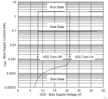 Figure 1. Bias Supply Current vs. Bias Supply Voltage
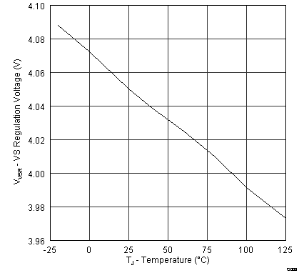 Figure 3. VS Regulation Voltage vs. Temperature
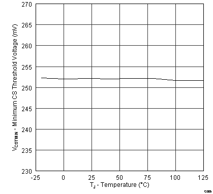 Figure 5. Minimum CS Threshold Voltage vs. Temperature

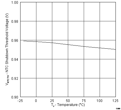 Figure 9. NTC Shutdown Threshold Voltage vs. Temperature
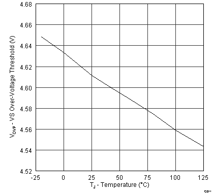 Figure 11. Overvoltage Threshold vs. Temperature
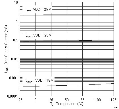 Figure 2. Bias Supply Current vs. Temperature
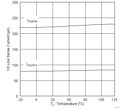 Figure 4. Line-Sense Current vs. Temperature
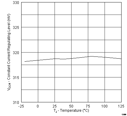 Figure 6. Constant-Current Regulating Level vs. Temperature
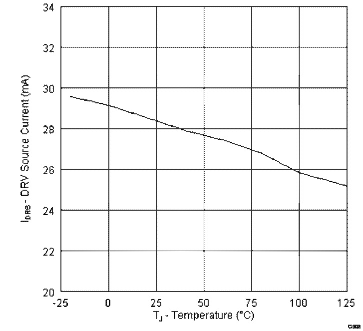
| VDRV = 8 V, VVDD = 9 V |
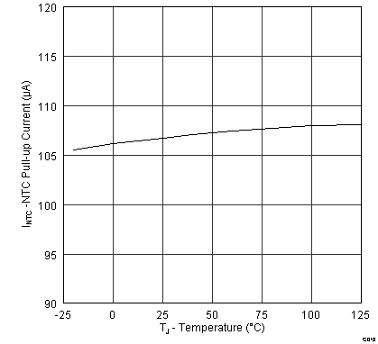 Figure 10. NTC Pullup Current vs. Temperature