Buffer Op Amp to Analog-to-Digital Converter Design: AC Coupled Single-Ended Input, Single Supply, Single-Ended Op Amps, Differential Input to ADC
Problem:
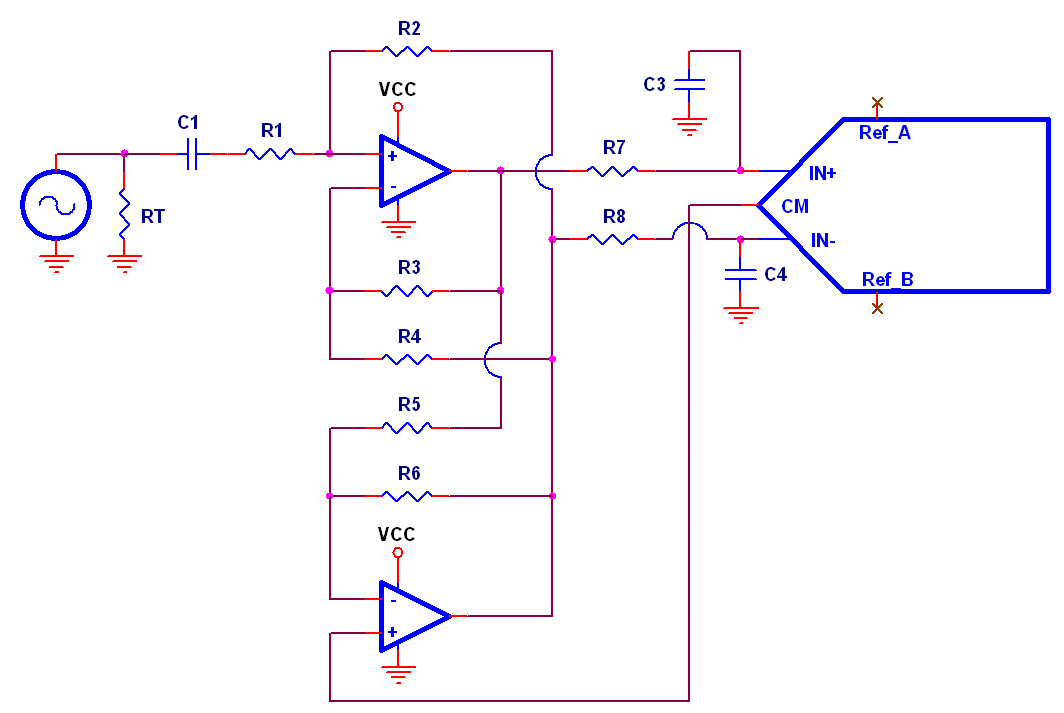
How do I buffer the input of an Analog to Digital Converter (ADC) when I have an AC coupled single-ended input, single power supply, single-ended op amps, and differential input to ADC?
Solution:

Double click on schematic to enlarge.
This implementation achieves fully differential output by cascading two inverting op amp stages. The top op amp with R3 and R4, forms the first stage. The second consists of the bottom op amp, R5
and R6. The overall circuit consists of an inverting gain stage consisting of input resistor R1, feedback resistor R2, and both op amps (with the bottom op amp performing the inversion for the top
op amp. To use this circuit, R3 through R6 should all be the same value and closely matched. R2 and R1 are the values required to set the gain of the circuit. R7, R8, C3 and C4 are ADC
compensation components.