Buffer Op Amp to Analog-to-Digital Converter Design: DC Coupled Single-Ended Input, Dual Supply, Single-Ended Op Amps, Differential Input to ADC
Problem:
How do I buffer the input of an Analog to Digital Converter (ADC) when I have an DC coupled single-ended input, dual power supply, single-ended op amps, and differential input to ADC?
Solution:
Double click on schematic to enlarge.
When the application calls for dc coupling, the your problems are multiplied. In ac-coupled applications, you only have to consider the ac gain of the stages. In a dc-coupled
application, the designer has to take the dc gain of the stages into account as well. The dc operating point and input common mode range of the op amps has to be considered, because dc gain can
easily upset it. Power consumption for high-speed dc coupled applications will probably be higher than in ac coupled applications, because common mode voltage levels to couple to ground through the
low value resistors normally found in high-speed applications. A problem related to this is the current that the common mode source has to provide may exceed the capability of the ADC.
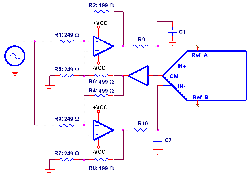
The schematic shows a specific application. The common mode source from the ADC is coupled to the op amps through a buffer stage. AC gain of the top stage is determined by R2 and R1, and is fixed
at 2. This gain is mirrored in the bottom stage, where gain is determined by R8 and R7. The non-inverting input of both the top and bottom op amps is presented with common mode reference, voltage
divided by 3 in resistors R6 and R5 for the top op amp, and resistors R4 and R3 for the bottom op amp. The dc gain of both op amps is the gain of a non-inverting op amp stage - in this case 3. The
dc common mode of the ADC is thus preserved at the op amp output, because its common mode output is divided by 3 in the voltage divider, and then multiplied by 3 in the non-inverting gain of the op
amps. R9, R10, C1, and C2 are the compensation components required by the ADC.