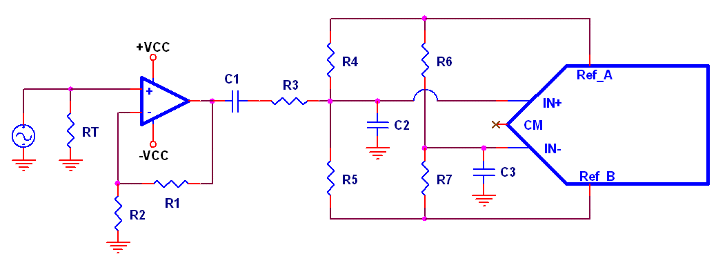
Buffer Op Amp to Analog-to-Digital Converter Design: AC Coupled Single-Ended Input, Dual Supply, Single-Ended Op Amps, Single-Ended Input to ADC
Problem:
How do I buffer the input of an Analog to Digital Converter (ADC) when I have an AC coupled single-ended input, dual power supply, single-ended op amps, and single-ended input to ADC?
Solution:


Double click on schematic to enlarge.
R1 and R2 are selected to provide non-inverting gain. C1 is a dc blocking capacitor. R3 and C2 are ADC compensation components. R4 through R7 are equal in value, and are used to provide a derived
common mode voltage to both the IN+ and IN- inputs. IN- is held at the common mode voltage, and bypassed by capacitor C3.

