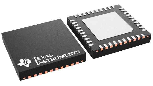
Packaging information
| Package | Pins WQFN (RSB) | 40 |
| Operating temperature range (°C) -40 to 105 |
| Package qty | Carrier 250 | SMALL T&R |
Features for the ADC3643
- Dual channel
- 14-bit 10/25/65 MSPS ADC
- Noise floor: –155 dBFS/Hz
- Ultra-low power with optimized power scaling: 29 mW/ch (10 MSPS) to 72 mW/ch (65 MSPS)
- Latency: 1 clock cycle
- 14-Bit, no missing codes
- INL: ±0.6 LSB; DNL: ±0.2 LSB
- Reference: external or internal
- Industrial temperature range: –40°C to +105°C
- On-chip digital filter (optional)
- Decimation by 2, 4, 8, 16, 32
- 32-bit NCO
- DDR and Serial CMOS interface
- Small footprint: 40-VQFN (5 mm × 5 mm) package
- Single 1.8-V supply
- Spectral performance (fIN = 5 MHz):
- SNR: 79.0 dBFS
- SFDR: 93-dBc HD2, HD3
- SFDR: 101-dBFS worst spur
- Spectral performance (fIN = 64 MHz):
- SNR: 74.0 dBFS
- SFDR: 84-dBc HD2, HD3
- SFDR: 90-dBFS worst spur
Description for the ADC3643
The ADC364x family of devices are low-noise, ultra-low power, 14-bit, 10-MSPS to 65-MSPS dual-channel, high-speed analog-to-digital converters (ADCs). Designed for low power consumption, these devices deliver a noise spectral density of –155 dBFS/Hz, combined with excellent linearity and dynamic range. The ADC364x offers very good dc precision, together with IF sampling support, which make the device an excellent choice for a wide range of applications. High-speed control loops benefit from the short latency of only one clock cycle. The ADC consumes only 72 mW/ch at 65 MSPS, and power consumption scales well with lower sampling rates.
The ADC364x use a DDR or serial CMOS interface to output the data offering lowest power digital interface, together with flexibility to minimize the number of digital interconnects. These devices are a pin-to-pin compatible family with different speed grades. These devices support the extended industrial temperature range of –40 to +105⁰C.