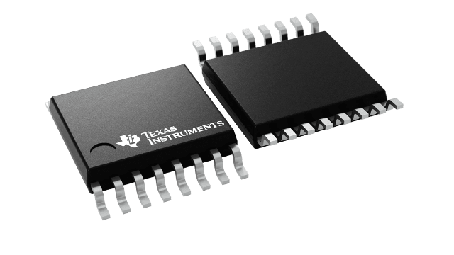
Packaging information
| Package | Pins TSSOP (PW) | 16 |
| Operating temperature range (°C) -40 to 125 |
| Package qty | Carrier 2,000 | LARGE T&R |
Features for the ADS8665
- 12-bit ADC with integrated analog front-end
- High speed:
- ADS8661: 1.25 MSPS
- ADS8665: 500 kSPS
- Software programmable input
ranges:
- Bipolar ranges: ±12.288 V, ±10.24 V, ±6.144 V, ±5.12 V, and ±2.56 V
- Unipolar ranges: 0 V–12.288 V, 0 V–10.24 V, 0 V–6.144 V, and 0 V–5.12 V
- 5-V analog supply: 1.65-V to 5-V I/O supply
- Constant resistive input impedance ≥ 1 MΩ
- Input overvoltage protection: up to ±20 V
- On-chip, 4.096-V reference with low drift
- Excellent performance:
- DNL: ±0.1 LSB; INL: ±0.15 LSB
- SNR: 74 dB; THD: –102 dB
- ALARM → high, low threshold
- multiSPI™ interface with daisy-chain
- Extended industrial temperature range: –40°C to +125°C
Description for the ADS8665
The ADS8661 and ADS8665 belong to a family of integrated data acquisition system based on a successive approximation (SAR) analog-to-digital converter (ADC). The devices feature a high-speed, high-precision SAR ADC, integrated analog front-end (AFE) input driver circuit, overvoltage protection circuit up to ±20 V, and an on-chip 4.096-V reference with extremely low temperature drift.
The devices operate on a single 5-V analog supply, but support true bipolar input ranges of ±12.288 V, ±6.144 V, ±10.24 V, ±5.12 V, and ±2.56 V, as well as unipolar input ranges of 0 V to 12.288 V, 0 V to 10.24 V, 0 V to 6.144 V, and 0 V to 5.12 V. The gain and offset errors are accurately trimmed within the specified values for each input range to ensure high dc precision. The input range selection is done by software programming of the device internal registers. The devices offer a high resistive input impedance (≥ 1 MΩ) irrespective of the selected input range.
The multiSPI digital interface is backward-compatible to the traditional SPI protocol. Additionally, configurable features simplify interface to a wide range of host controllers.
