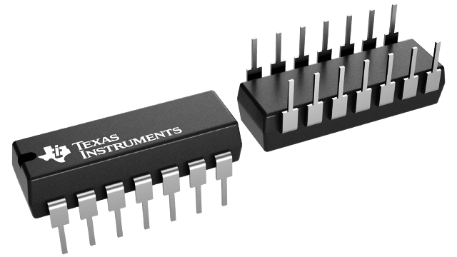
Packaging information
| Package | Pins PDIP (N) | 14 |
| Operating temperature range (°C) -55 to 125 |
| Package qty | Carrier 25 | TUBE |
Features for the CD4007UB
- Standardized symmetrical output characteristics
- Medium Speed Operation — tPHL, tPLH = 30 ns (typ.) at 10 V
- 100% tested for quiescent current at 20 V
- Meets all requirements of JEDEC Tentative Standard No. 13B, "Standard Specifications for Description of ’B’ Series CMOS Devices"
- Maximum input current of 1 µA at 18 V over full package-temperature range; 100 nA at 18 V and 25°C
- Applications:
- Extremely high-input impedance amplifiers
- Shapers
- Inverters
- Threshold detector
- Linear amplifiers
- Crystal oscillators
Data sheet acquired from Harris Semiconductor
Description for the CD4007UB
CD4007UB types are comprised of three n-channel and three p-channel enhancement-type MOS transistors. The transistor elements are accessible through the package terminals to provide a convenient means for constructing the various typical circuits as shown in Fig. 2.
More complex functions are possible using multiple packages. Numbers shown in parentheses indicate terminals that are connected together to form the various configurations listed.
The CD4007UB types are supplied in 14-lead hermetic dual-in-line ceramic packages (F3A suffix), 14-lead dual-in-line plastic packages (E suffix), 14-lead small-outline packages (M, MT, M96, and NSR suffixes), and 14-lead thin shrink small-outline packages (PW and PWR suffixes).
